What Does Quickturn PCB Mean?
When engineers need to get a prototype of a PCB manufactured in a short space of time, they often require a service that is able to accelerate manufacturing without compromising quality. While it is possible for prototype PCBs to be hand soldered, the increasing miniaturization of components such as BGA and MLF makes this an impractical and time-consuming approach, especially for those who do not have expertise in such techniques. Thus, engineers will often turn to PCB assembly services that specialize in mass production, even for individual prototypes.
However, the use of such services introduces multiple manufacturing considerations, including component sourcing and fabrication. Unlike standard manufacturing runs, prototypes in mass can rely on low-volume manufacturing techniques, but this introduces the risk of increased manufacturing errors. At the same time, the low volumes can also result in component availability issues, something which is outside the control of the engineer.
Therefore, engineers requiring quick turn PCBs for prototyping need to turn to manufacturers that not only have expertise in fast manufacturing, but also in component sourcing. This is where US-based manufacturers can provide engineers with a superior service, not just with regards to delivery times but also with regards to quality.
The reliance on digital processes also allows such manufacturers to rapidly orchestrate the entire supply chain, including logistics, which can help to reduce the time taken for a prototype to be manufactured and delivered. In the case of our quick turn PCB service, engineers can get custom PCBs delivered in as little as six days, providing engineers with a rapid manufacturing service that is focused on time-critical projects.
Benefits of a Quickturn PCB
Engineers are always pushed against time whether it is due to other projects taking priority, the need for multiple prototypes to be manufactured, or simply because a product needs to be to market before a competitor. In the case of PCB fabrication and assembly services, the ability to have a fully built and tested circuit board in a short period of time allows engineers to accelerate their projects significantly.
The fast turnaround of a PCB also allows for engineers to continue their line of thinking without being interrupted by long delays in prototype manufacturing. Furthermore, earlier prototypes also allow for testing and debugging at earlier stages, and this in turn helps to reduce the overall amount of time needed to get a project from concept to reality.
In fact, the ability to receive prototypes earlier also gives engineers the ability to make design changes faster, and these changes can then be incorporated into new prototypes. Thus, for the same amount of time, quick turn PCBs allow for more innovations to be integrated into a product.
Factors That Impact the Timeframe of a PCB Prototype
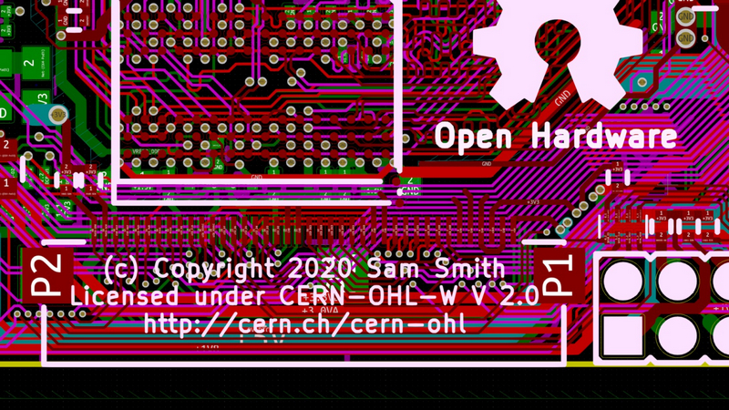
When it comes to the manufacture of a PCB, by far the biggest cause of error is the submission of a design that is riddled with errors. These errors can include trace widths being too narrow or too wide, placement of parts that may conflict with each other, and some parts being impossible to source.
Unfortunately, many of these types of errors cannot be identified via software, meaning that it is only once a manufacturer receives a submitted design that they can start to identify potential issues. Once identified, manufacturers can then inform engineers of the problems, but this can lead to massive delays in manufacturing. For example, a part that is found to have a trace width that is too narrow may require a redesign, and this could see a two-day delay in manufacturing time.
The second major challenge faced with manufacturing PCBs is ensuring that all components are readily available. A PCB that is submitted for manufacture can only be manufactured if all the components required by the PCB are in stock. If any of these components are unavailable, the entire production run will be held up, waiting for these components to become available.
In some cases, components that are on backorder inside the US may be available in quantity from the far east. However, as these parts will need to be shipped to the US, not only are there extremely long delay times in shipping and customs clearance, but the cost of delivery can be extortionate.
Finally, it is also essential that the most up to date version of a project is submitted to the manufacturer. A project that has undergone numerous changes will only work if the Bill Of Materials (BOM) and the design file refer to the same project. If these two do not match, then manufacturing can be significantly delayed while engineers and manufacturers try to figure out why component positions are not correctly matching with the PCB design files.
Factors to Consider When Looking
When needing to get a PCB manufactured, it is essential that engineers consider the manufacturer they choose, especially if the part is needed urgently. For example, some PCB manufacturing services may be located in far-off places such as China, and while this may be economical, it can also see long delays in manufacturing and shipping.
Choosing a manufacturer that is closer to home can be highly beneficial, and not only helps to reduce manufacturing times but also helps out the local economy. However, simply picking any local PCB fabrication service is not enough; many factors still need to be taken into consideration.
Firstly, it is imperative that the local manufacturer has access to a wide range of parts so that no component of the design holds back manufacturing. For example, DigiKey and Mouser Electronics are two major authorized component distributors who have access to most components on the market, and a PCB manufacturer having access to either one means that the manufacturer will unlikely fall into component sourcing issues.
Secondly, it is also critical that the manufacturer follows recognised quality standards such as ISO 9001. This helps to ensure a consistent manufacturing process and checks for quality at each stage of the production process.
Thirdly, it is important to also understand the delivery terms offered by the manufacturer so that customers know what to expect. For example, some manufacturers may offer a 24-hour delivery service for those in the local area, while others may take a few days.
Finally, those working with cutting-edge designs where IP protection is of the utmost importance will also need to check the manufacturer’s cybersecurity standards. With the many advances in technology, it is not uncommon for designs to incorporate sensitive information such as network credentials or decryption keys. As such, it is essential that the manufacturer has strong cybersecurity measures to prevent such information from being leaked.
By taking these simple steps, engineers can ensure a high-quality manufacturing process that produces reliable circuits in a short time while also protecting their IP.
How to Get a Quickturn PCB Prototype
When it comes to getting a prototype PCB manufactured, it is essential that engineers take steps to ensure that their design conforms to the capabilities of the manufacturer while also being mindful of other factors that may affect the final design. For example, trace widths and spacings must be taken into account as well as drill sizes and the number of layers as this will not only affect the final design but also the price.
Before starting a project, engineers should also consider the space between traces and the edge of the PCB as well as component courtyards and minimum feature sizes for component legend items. While these may not be essential for a prototype, future designs will likely be mass produced, and these tiny details can make a world of difference.
Once a prototype has been designed and the schematic verified, it is time to choose a manufacturing service. The first step in this process is to create a list of potential services that are capable of producing the circuit in question. From there, engineers should contact each service and go through a series of questions to ensure that they understand their process as well as their level of customer support.
Check out our free email template so you can get answers to your questions fast!
Creating a relationship with a manufacturer can also be beneficial for engineers as it can help to understand how to approach the manufacturer should issues arise. Furthermore, it also allows engineers to better understand the workflow and how their design will be handled throughout the manufacturing process.
After a list of potential manufacturers has been curated, engineers can then rank the services based on their capabilities and work ethic. In the case of a US-made quickturn PCB, the focus would be on fast manufacturing and high-quality results.
Our Process for Fast PCB Manufacturing
When it comes to getting custom PCBs fabricated and assembled, time is often of the essence, especially when working on projects that are the sole focus of a company. For example, electric vehicle developers often need to move as fast as they need to be at the forefront of the industry, and medical device manufacturers must ensure that their designs conform to strict regulations, which incurs extremely long testing schedules and qualifications.
Engineers using our PCB fabrication and assembly services can rest assured that our many years of combined experience mean that we have most likely seen the problems that your project will encounter, and our engineers are not only knowledgeable on how to handle these challenges, but will work with you to ensure that your designs fabricate and function correctly. Of course, as we cannot predict every possible decision that an engineer could make (such as running data lines through power rails), we cannot guarantee that a design will function as expected.
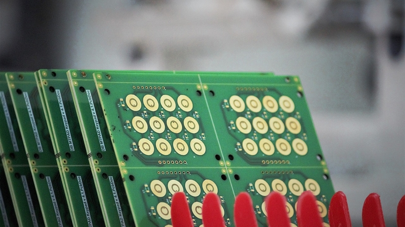
To get custom PCBs from us, engineers simply need to submit their PCB design files, clearly stating what their design requires, how many are needed, and the required delivery time. From there, our engineers will provide a quote, which, once paid, will trigger our software-powered systems to manufacture PCBs that will then be delivered to customers within 6 days.
As our US-based services are ideal for those needing quick-turn PCBs, we offer delivery options that are second to none. For those in the Oakland area, it is possible for boards to be hand-delivered by our founder Derek Elley, and all customers can expect delivery of their custom PCBs within 24 hours of their completion. By choosing our quick PCB fabrication and assembly services, engineers can focus on the aspects of their project that require their attention, and leave the manufacture and delivery of parts to our team of experts.
Why Choose Ponoko
When requiring prototypes or low-volume production of circuit boards, many engineers face numerous challenges in selecting the right manufacturer. Not only are there many potential options available, but even within the US, there are numerous manufacturers that can make custom PCBs, each with their own set of capabilities.
Trying to compare the various manufacturers can be challenging, as some focus on specific aspects of a design. However, Ponoko is a unique manufacturer in that it not only specializes in PCB design and assembly but also other related processes, including laser cutting and 3D printing. This means that Ponoko is able to take a prototype PCB and turn it into a physical product, including enclosures, gaskets, faceplates, and packaging.
The years of experience that Ponoko has in the field also means that Ponoko is able to recognize the importance of both PCB design and the final product. This means that engineers can leverage the expertise of Ponoko to help with any challenges faced during product development, whether it is a new PCB or a new product.
An important aspect of Ponoko services is that all PCBs and assembled PCBs come with a 365-day guarantee, providing engineers with a level of protection rarely seen from other manufacturers. Furthermore, Ponoko has manufactured over 2 million products for more than 35,000 customers, resulting in a precision part rate of 99.3%, demonstrating the reliability and capabilities of Ponoko.
As Ponoko offers numerous manufacturing services, including injection molding, laser cutting, and 3D printing, engineers can use Ponoko for both prototyping and mass production. This means that products can continue using Ponoko services as they scale, eliminating the need to find new manufacturers.
Finally, Ponoko holds numerous international standard qualifications, including ISO 9001, ISO 13485, and ITAR, ensuring that all parts produced conform to strict quality parameters and are suitable for any market around the world. The combination of these qualifications and Ponoko’s guarantee provides engineers with a manufacturing partner that is reliable, professional, and dependable.
