What is a PCB?
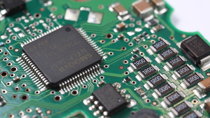
Printed Circuit Boards (commonly abbreviated as PCBs) are fundamental components in virtually all electronic devices. They are constructed using multiple layers of copper, which are crucial in creating interconnections among various electronic components. These copper layers are meticulously designed to ensure that electricity can flow between components such as resistors, capacitors, and integrated circuits in an efficient and controlled manner.
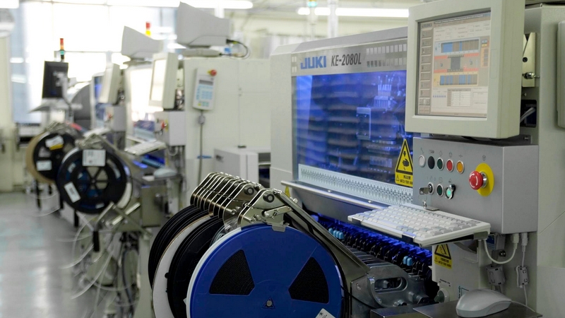
The process of assembling these components onto the PCB is precise. Components can be attached to a PCB using one of two methods: through-hole or surface-mount technology (SMT).
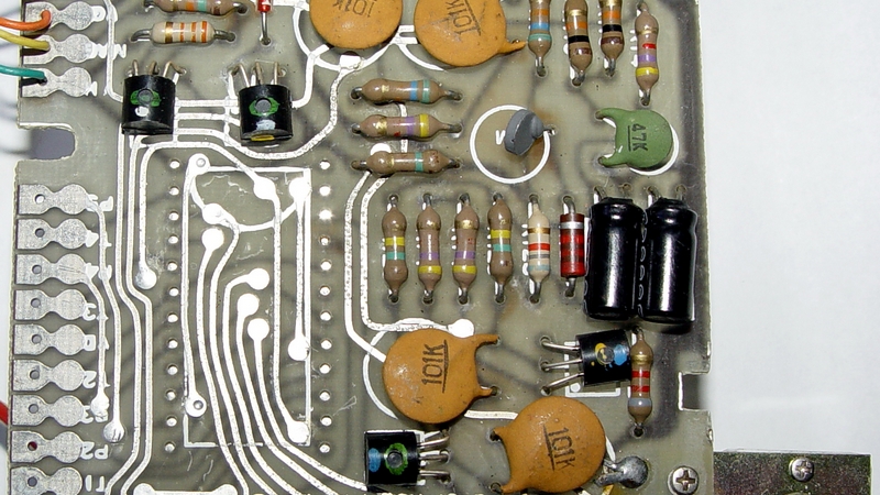
- Through-hole technology involves inserting the leads of components through pre-drilled holes in the PCB, which are then soldered to pads on the opposite side. This technique provides strong mechanical bonds but is generally bulkier and slower compared to its counterpart.
- Surface-mount technology (SMT), on the other hand, involves mounting components directly onto the surface of the PCB. This method allows for more components to be mounted on both sides of the board, making SMT the preferred technique for modern compact electronic devices due to its efficiency and ability to support higher circuit densities.
The term “printed” in Printed Circuit Boards arises from the manufacturing process used to create these boards. Techniques such as silk-screening, photo imaging, and developing are employed to precisely apply a protective mask, which outlines where copper and other materials should be placed or removed.
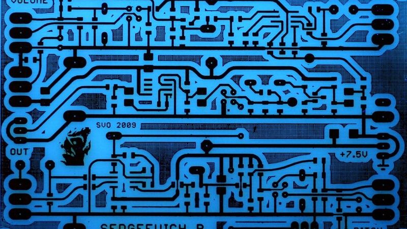
Silk-screening, for instance, is a process where ink is pushed through a stenciled mesh screen to create a printed pattern on the PCB. This pattern forms the protective mask that defines the layout of the circuit, including where connections should and should not occur.
PCBs are crucial because they are used in every electronic circuit on the market today. From consumer electronics like smartphones and televisions to critical medical equipment and automotive components, PCBs form the backbone of these devices. Without PCBs, the intricate and compact circuits necessary for today’s technology would not be possible, rendering modern conveniences such as mobile computing and instant communication impractical, if not impossible.
PCBs are also critical in the development of new technologies such as the Internet of Things (IoT), which involves the connection of millions of devices via the internet. Such technologies would not be possible without PCBs. The ability to create custom designs with ease and high precision makes PCBs essential in the prototyping of new circuits and designs.
Despite the sophistication and critical role of PCBs in modern electronics, they are surprisingly not difficult to produce. Advancements in technology and manufacturing processes have significantly streamlined PCB production, making it highly efficient and cost-effective. The industry has mastered the art of mass-producing these boards with high precision and at low costs. This efficiency has been pivotal in reducing the cost of electronic devices while simultaneously increasing their availability and reliability.
PCBs Now & Then (Past & Present)
Printed Circuit Boards (PCBs) have seen a remarkable evolution since their initial development, transforming from simple designs to complex multi-layered components crucial in modern electronics.
Early Development
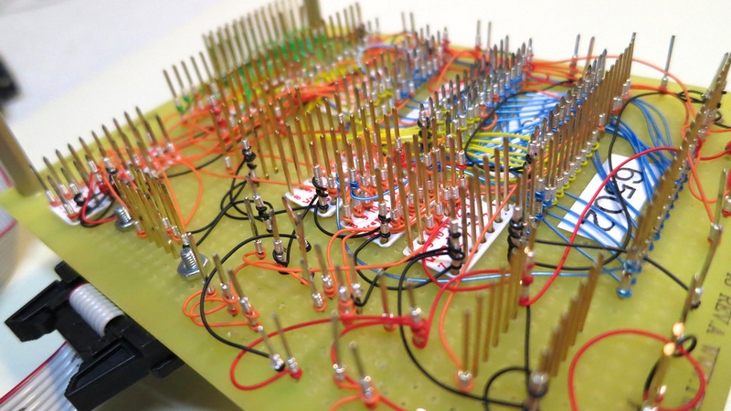
Initially, before the advent of PCBs, electronic circuits were manually assembled on wooden boards—often kitchen breadboards. These early versions involved attaching electronic components directly onto the board and connecting them with wires soldered together. This rudimentary method was not only time-consuming but also prone to errors and failures, leading to the need for more reliable and scalable solutions.
As technology progressed, wire-wrap techniques became popular. This method involved wrapping wires around the legs of components to form connections, offering a slightly more durable and reproducible technique compared to direct soldering on breadboards. However, the limitations in scalability and the labor-intensive process of wire-wrapping led to the pursuit of more advanced manufacturing techniques.
World War II and the Birth of PCBs
The real breakthrough came during World War II when the U.S. military faced significant challenges in manufacturing reliable proximity detonators. The military’s need for robust, mass-producible electronic circuits led to the development of the first PCBs. Those early PCBs were crafted from Bakelite, a type of plastic, and featured a single layer of copper for conducting paths. Although basic in design, these boards marked a pivotal shift towards standardized electronic components.
Post-War Advancements
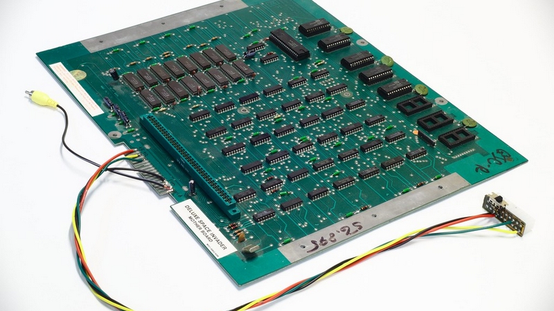
Over time, PCBs underwent numerous enhancements. Manufacturers began adding multiple layers of copper to accommodate more complex circuits within compact spaces. The introduction of solder masks helped protect the copper from oxidation and prevented solder bridges between closely spaced conductors. Silkscreens were also added to the PCBs, providing labels for component placement, which facilitated easier and more accurate assembly.
Another significant advancement was the development of through-hole plating. This technology allowed for the connection of multiple layers within the PCB through plated holes known as vias. This capability enabled designers to create more complex and dense circuit configurations, enhancing the functionality of electronic devices.
Modern PCBs
The evolution of PCB manufacturing technologies continued with improvements in lithographic techniques and printing materials. These advancements allowed for finer traces, smaller drill holes, and the accommodation of faster signal transmissions—crucial as electronic devices became increasingly sophisticated.
Today, modern PCBs are marvels of engineering, capable of having up to 32 copper layers. They include features such as internal vias and pads that connect directly to the dies of semiconductor chips, supporting the high-speed, high-density requirements of contemporary electronic devices. The ongoing innovation in PCB design and manufacturing continues to drive the development of smaller, faster, and more efficient electronic devices.
Types of Printed Circuit Boards
Single-sided PCBs were the norm in the past, consisting of a single layer of conductive copper material. Their simplicity made them popular in early electronic devices, and they are still used in some basic applications such as sensors and relays. However, their simplicity is also a limitation, restricting their use in modern, multifunctional devices.
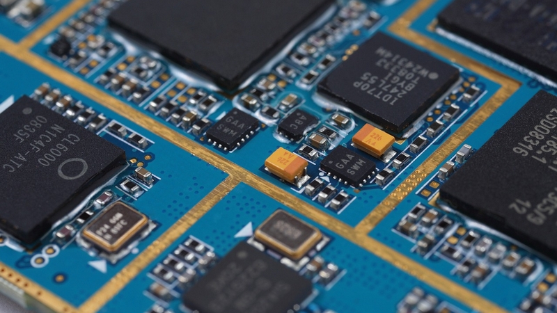
As technology advanced, the demand for more compact and complex electronics grew, and double-sided PCBs emerged. These boards feature conductive copper layers on both sides, allowing for a denser arrangement of circuits, and often have plated-through holes that allow for electrical connections between the two sides. This design significantly expands the potential for more complex circuits and is why double-sided PCBs are commonly found in consumer electronics, mobile devices, and personal computers.
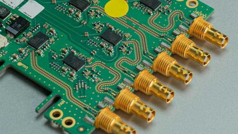
For even more complex systems, engineers turn to multi-layer PCBs which consist of three or more layers of copper, with each layer separated by a substrate layer. These boards can have as many as twelve layers or more, and the use of multiple layers allows for a much denser routing of circuits. Multi-layer PCBs are essential in applications that require a high degree of signal integrity, such as RF communication and high-speed digital signals, and are commonly found in GPS technology, satellite systems, and advanced communication devices.
Another innovative type of PCB is the flexible PCB which uses a flexible substrate material such as plastic. These boards can bend and flex during use, making them ideal for applications that involve movement or vibration. As such, flexible PCBs are commonly found in modern wearable technology, flexible displays, and automotive electronics.
Each type of PCB brings its own set of capabilities and advantages, catering to a wide range of applications and ensuring that electronic devices continue to become smaller, faster, and more complex.
Structure of PCBs
The electronics industry is reliant on the ability to create increasingly complex circuits, and the use of PCBs allows for engineers to achieve this with ease. At the heart of a PCB is the dielectric material which provides structural support, is the base for other layers, and also helps to insulate different conductive layers.
While FR4 fiberglass is a popular choice for dielectric materials due to its flame resistance and high dielectric strength, other materials can be used depending on the application. For example, flexible PCBs may use a paper epoxy blend to allow for bending and warping while ceramic can be ideal for use in environments exposed to high temperatures. Glass can also be used in applications that require a high degree of reliability and long-term reliability such as in space missions.
The next layer in a PCB includes the copper conductors that allow for electrical current to flow through the PCB. These layers are typically 1oz copper which is 35 microns in thickness, but this can vary depending on the current requirements of the circuit. The importance of these layers cannot be understated as they enable components to interact with each other and allow for the circuit to perform its intended function.
To protect the copper layers, a solder mask is applied that prevents oxidation as well as preventing solder from spreading to areas where it is not needed. While the solder mask may seem like an optional layer, it is in fact a critical component of a PCB as solder that breaches the mask can damage copper layers and prevent proper soldering during the manufacturing stage.
The final layer of a PCB is the silkscreen which is used to add graphics and text to the PCB. While this layer may seem like an afterthought, it plays a critical role during the manufacturing stage as it helps guide components into their correct position. The use of a silkscreen also allows for custom designs to incorporate company logos and other designs to make PCBs more unique.
The Process of Printed Circuit Board Design
The automation of PCB design has significantly reduced the time spent on design and manufacturing while increasing accuracy and reducing the likelihood of errors. However, the development of a PCB requires a comprehensive understanding of the entire process to ensure the success of the project. The use of Electronic Computer-Aided Design (ECAD) tools, such as KiCAD, is essential for creating efficient and reliable circuit boards. These tools provide a collaborative environment for engineers to design, prototype, and test their circuits effectively.
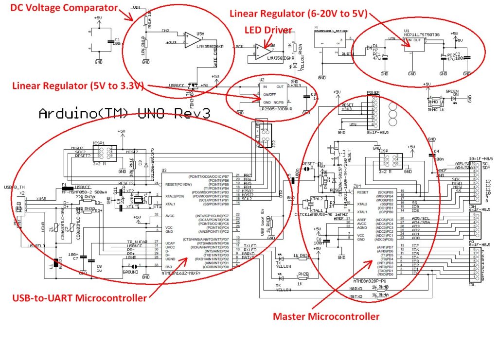
The design process begins with the creation of a schematic diagram that shows all the components and their connections. This blueprint of the circuit helps engineers review the design and identify potential errors early, ensuring that the final product is functional and efficient. The schematic also serves as a basis for creating a Bill of Materials (BOM) that lists all the components needed for the circuit, which is essential for prototyping and manufacturing the PCB.
In the PCB layout stage, engineers place components on the board and route the traces that connect them. This stage requires careful planning to ensure that the PCB is manufacturable, as well as to optimize the performance of the circuit. The use of automation tools helps engineers route traces efficiently, but manual intervention is still necessary to ensure that the design is practical and free from potential issues.
After the PCB has been designed and checked for errors, engineers can order prototypes or undergo final manufacturing. The prototyping stage is crucial for testing the functionality and performance of the circuit, and the low cost of prototypes enables for rapid prototyping and testing. The high degree of accuracy and precision of CAD tools ensures that prototypes match the final product, reducing the time and cost of product development.
How to Create Your Own PCB Design
Creating a PCB can seem like a daunting task given its complexity and the precision required in designing one. However, this should not deter aspiring designers and hobbyists from delving into the world of electronics design. PCB design is a skill that can be mastered with patience and the right resources.
For those who are new to PCB design, the first and most crucial step is choosing the right software. KiCAD is an excellent option for those who are new to PCB design as it is free and open-source. Unlike many commercial software options that come with high costs, KiCAD offers a cost-effective solution without compromising on functionality. It supports all the features needed for designing professional-quality circuit boards, from schematic capture to PCB layout, and is complemented by a wealth of online resources and tutorials.
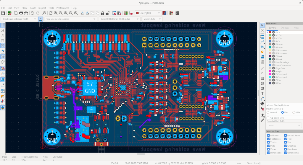
These tutorials are invaluable for beginners, covering everything from basic concepts of schematic capture to part selection, where designers choose the electronic components that will be used in the circuit. Learning how to navigate these initial steps is crucial, as they form the foundation of PCB design.
For those who have experience in PCB design, software tools like Eagle and Altium are popular among professionals due to their advanced features and capabilities. Eagle is known for its user-friendly interface and strong community support, while Altium is favored for its robust design features and integration capabilities. While these tools are popular among professionals, it is important to recognize the strides that KiCAD has made over the years. It has evolved significantly and now offers functionalities that are on par with its commercial counterparts, making it a cost-effective option for those who require powerful design tools without the associated costs.
Whether one is a beginner or an experienced engineer, there is a range of software options available to suit various needs and budgets. KiCAD stands out as a particularly strong option for those starting out, providing all the necessary tools for free. With the availability of comprehensive tutorials and a supportive community, anyone motivated to learn can acquire the skills needed to design their own PCBs.
Key Takeaways
Printed Circuit Boards or PCBs are fundamental components in the electronics industry serving as the backbone for assembling various electronic components into a functional circuit. A PCB features a board made of non-conductive material typically fiberglass or plastic which supports and connects a variety of electronic components through conductive pathways pads and other features etched from copper sheets laminated onto the substrate. These traces are essential as they form the circuit by providing a pathway for power and signals between the physical components.
The complexity of PCBs can vary significantly depending on their application; some PCBs are simple and contain only a single layer of conductive material ideal for basic devices like a calculator. On the other hand, advanced systems such as computer motherboards or satellite systems may require a PCB with up to 32 layers. These multilayer boards are beneficial for complex electronic systems providing more space for the conductive traces and the ability to manage electromagnetic interference more effectively.
When it comes to attaching components to PCBs there are primarily two methods: surface-mount technology SMT and through-hole technology. SMT involves soldering components directly onto the surface of the PCB which allows for more components to be mounted on a given area of the board thus reducing the PCB’s overall size and weight this method is prevalent in modern electronics manufacturing. Through-hole technology on the other hand involves inserting the leads of components through pre-drilled holes in the PCB and then soldering them in place. This technique is often used for components that require stronger physical connections with the board such as connectors that undergo frequent plugging and unplugging.
Designing PCBs is a sophisticated process that utilizes Electronic Computer-Aided Design ECAD tools. These software tools assist engineers in creating the layout of a PCB including the placement of components and the routing of electrical connections. KiCAD is one such ECAD tool that is widely recognized for its capability and versatility in PCB design. It is an open-source software that provides engineers with a comprehensive suite of tools to develop PCBs from concept to production.
The design process itself involves several critical steps initially engineers perform schematic capture which is the creation of a schematic diagram that represents the circuit in symbols and connections this schematic serves as a blueprint for the PCB layout following this component selection is carried out where each part is chosen based on its performance characteristics and compatibility with other components the arrangement of these components on the PCB is then planned to optimize the design and improve its performance finally the PCB is routed to create the electrical connections between components and the board is manufactured.
Why Choose Ponoko
At Ponoko, we pride ourselves on being more than just an electronic assembly fabricator. We offer a comprehensive range of manufacturing services, including laser cutting, CNC milling, and injection molding. This extensive variety allows us to produce all the necessary components for your project under one roof, significantly accelerating prototype development and ensuring a seamless production process.
By choosing Ponoko as your single manufacturer, you benefit from a streamlined production process where all parts are guaranteed to be compatible and adhere to the same high-quality standards, minimizing the risk of project delays. Communication is also simplified, with a single point of contact providing clear and consistent updates throughout the entire project lifecycle.
Our commitment to precision and quality is unmatched, with a precision part rate of 99.7% across over 2 million parts produced for our 33,000-strong customer base. This level of accuracy is critical for the functionality of your PCBs, ensuring that every component fits and operates as intended.
Ponoko’s manufacturing capabilities are designed to support both prototypes and mass production, making us your ideal one-stop solution for product development. Additionally, our ability to produce custom components and assemblies helps protect your intellectual property, as these unique parts are exclusively available through Ponoko.
With Ponoko, you gain not just a manufacturing partner, but a comprehensive solution that supports every stage of your product’s journey, from concept to production.
FAQs
- What are Printed Circuit Boards (PCBs)?
- PCBs are fundamental components in modern electronic devices, used in everything from simple gadgets to complex machinery.
- What are the main stages in the creation of a PCB?
- The process is divided into two main stages: fabrication and assembly.
- What does PCB fabrication involve?
- PCB fabrication includes creating the circuit board itself, etching the copper layer to form traces, drilling holes for mounting components, and applying a protective mask to prevent short circuits.
- What is PCB assembly?
- PCB assembly is the process of mounting electronic components onto the fabricated board, which can be done through methods like surface-mount technology (SMT) or through-hole technology.
- What services does Ponoko offer for PCBs?
- Ponoko offers PCB fabrication, allowing designers and engineers to turn their electronic circuit designs into physical boards. Ponoko also offers PCB design services to help optimize designs for fabrication.
- What types of PCBs does Ponoko offer?
- Ponoko offers a variety of PCB types, including single-sided, double-sided, and multi-layer PCBs, catering to different needs and applications.
- Does Ponoko offer advanced PCB design services?
- Yes, Ponoko offers PCB design services, especially beneficial for those without in-house expertise, ensuring the design is optimized for fabrication and meets all necessary specifications.
- What materials does Ponoko offer for PCB fabrication?
- Ponoko offers a range of standard and high-speed PCB materials, allowing customers to choose the best material for their design based on factors like manufacturing speed, cost, and high-frequency signal integrity.


