

"Hello! I received my order yesterday, exactly when promised. Please extend my thanks to the entire Ponoko team. I'm thrilled with the work you have done, the quality exceeds my expectations and is better than work I'd done previously myself in the local lab. Very impressed, I'll be ordering again, thank you!"
Board capabilities
Surface finish
Copper to board edge clearance
Board area
Board thickness
• Thickness < 1.0mm: ±15%
• Thickness > 1.0mm: ±10%
Layer count
Fabrication process
Dielectric material families
Controlled impedance layers
Quality Inspection
Holes & vias capabilities
Drill and mill
Mechanical drill diameter
Laser drill diameter
Mechanical through via aspect ratio
Vias
Via fill
Laser blind via aspect ratio
Copper capabilities
Minimum annular ring width
Drill to trace clearance
Drill to plane clearance
Trace & space
Soldermask & silkscreen capabilities
Solder
Soldermask colors
Soldermask dam
Minimum soldermask pad relief
Silkscreen colors
Minimum silkscreen size
Mechanical limits
Chip components: resistors / capacitors 01005
Leaded packages: SOIC/QFP/TSOP lead pitch
Leadless packages: QFN, TQFN lead pitch
BGA: BGA/FBGA/LGA ball pitch
Our PCB assembly capabilities
Our PCB assembly capabilities support SMT components with a minimum BGA pitch of 0.35mm, CSP components, and both SMT and through-hole technologies. Lead times for our services are a minimum of 6 days, and order quantities vary from 1 to 1 million. Additionally, all our assembled boards conform to ISO-9001, UL-796, IPC-6012, IPC-A-610, and ITAR standards.
- Components sourced from US / global suppliers
- Single or double sided
- Through-hole
- SMD
- BGA
- LGA
- PTH
- Hybrid
- SoP
- Daughterboard components
- Modules
- Cable & wire harness
- 01005 10 mil x 05 mil
- Full product assembly & box build
- IPC-A-610 ESD
What is PCB fabrication & assembly?
Our PCB fabrication and assembly service is a one-stop solution for engineers needing to manufacture electronic devices, which includes PCB fabrication, component sourcing, and final assembly. Traditionally, these services are often separated, making it difficult for engineers to organize as blank PCBs have to be shipped to an assembly service while simultaneously needing to source components suitable for use in automation equipment (such as pick and place). By combining all these processes into a single service, engineers can spend more time on product development while our software-driven solutions intelligently orchestrate the entire supply chain to produce fully populated, high-quality circuits.
Our PCB fabrication & assembly services start with the manufacture of PCBs. Customer designs are checked for potential design errors that may conflict with our manufacturing processes. Once designs have been confirmed, manufacturing files are produced that include CNC drill files and transparent plots for layer imaging. Using a series of different manufacturing steps, layers are drilled, plated, imaged, and then laminated to create traces and vias. The final step in PCB fabrication involves the application of solder masks, component legends, and surface finishes such as HASL and gold.
Once the PCB has been fabricated, it is sent to our assembly facilities which use pick-and-place machines to place components automatically. Depending on the component being placed, these fully automated machines can use multiple placement heads to position up to 15 components per second. After all the parts have been placed, the PCB is then sent through a reflow oven which solders all components simultaneously. During this stage, it is essential that the heat of the reflow oven is separated into zones with varying temperatures so as not to damage components, the PCB, and ensure high-quality solder joints.
Finally, PCBs undergo automatic optical inspection (AOI) to guarantee the quality of solder joints, the position of components, and to identify any potential damage during manufacture. The high speed of AOI enables boards to be rapidly imaged and checked without needing to rely on human labor, thus reducing costs and increasing production rates.
How does digital manufacturing work?
It’s no secret that PCB fabrication, component sourcing, and assembly can be tricky to get right, especially if an assembly service has specific PCB requirements, or won’t accept certain types of component reels. Worse, trying to source components from numerous distributors and coordinate different orders can be a nightmare for both engineers and PCB assembly services alike.
To help engineers with this, Ponoko has developed an entirely digital manufacturing service that separates design engineers from manufacturing processes, including part ordering and sourcing. In addition to this, our digital manufacturing also connects our assembly sites with distributors over a single network that provides real-time communication and order placement. The moment a PCB is ready for manufacture, the component list is checked against our partnered distributors, and the best price is obtained while simultaneously organizing the entire order process.
In addition to logistics management, our digital manufacturing services also provide tools for engineers to get rapid quotations. This removes the need for engineers to get numerous quotes for complex supply chains that can often take weeks.
How much does PCBA assembly cost?
Due to the countless options and variations associated with PCBs, there is no one single answer for their cost. However, the four main factors that affect the price of PCB assembly services include the size of the PCB, the number of layers used, the total number of components being assembled, and whether there are any components that cannot use automation processes.
For example, basic 2-layer PCBs that use a handful of commonly used SMD components will be very cheap, but larger PCBs with more than four layers and hundreds of SMD components will be more expensive. In addition, engineers should also try to avoid components that are not compatible with automation processes (such as some connectors and wires), as these require manual soldering, which is a time-consuming process (and thus faces significant labor costs).
Hardware quality, at software speed
The two largest factors that affect manufacturing processes are quality and speed, and increasing one usually results in the loss of the other. However, thanks to our digital manufacturing capabilities, we are able to offer industry-leading quality assembled PCBs, approaching software speeds. As our digital manufacturing process utilizes software to orchestrate PCB fabrication with component sourcing and assembly, quotation times and logistics are massively reduced, while logistical optimisation ensures continuous production.
But to really demonstrate confidence in our software-driven manufacturing services, all assembled PCBs come with a 365-day guarantee which provides engineers with a level of protection rarely seen from other manufacturers. In addition to this guarantee, we have manufactured over 2 million products for over 35,000 customers, and with a precision part rate of 99.3%, there is a reason why ambitious engineers choose Ponoko.
What is PCBA used for?
The importance of electronics in daily life sees PCB fabrication and assembly used in every industry across the planet. Whether it is desktop PCs, kitchen appliances, medical devices, or IoT sensors, wherever electronics are found, PCBA is almost guaranteed to be used. The automated nature of PCBA makes it extremely economical, and the development of automatic optical inspection and probe testing enables most quality controls to be done by computer, further making PCBA highly efficient.
And unlike many other manufacturing processes, PCBA is used for both prototyping and mass production because the manufacturing process is identical. Of course, prototypes can be hand soldered, but the move towards extremely small SMT parts such as BGA and MLF makes hand soldering impractical and time-consuming. Thus, engineers opt for PCBA, even if only a handful of boards are needed.
With regards to some of the most popular industries, the IoT and computer industries are the most involved with PCBA as they are, by nature, entirely electronic. The medical industry has also come to rely on electronics thanks to the developments in sensor technologies, and the automotive industry has become mostly dependent on electronics for engine control, safety monitoring devices, and the introduction of EVs.
Smart IoT sensors
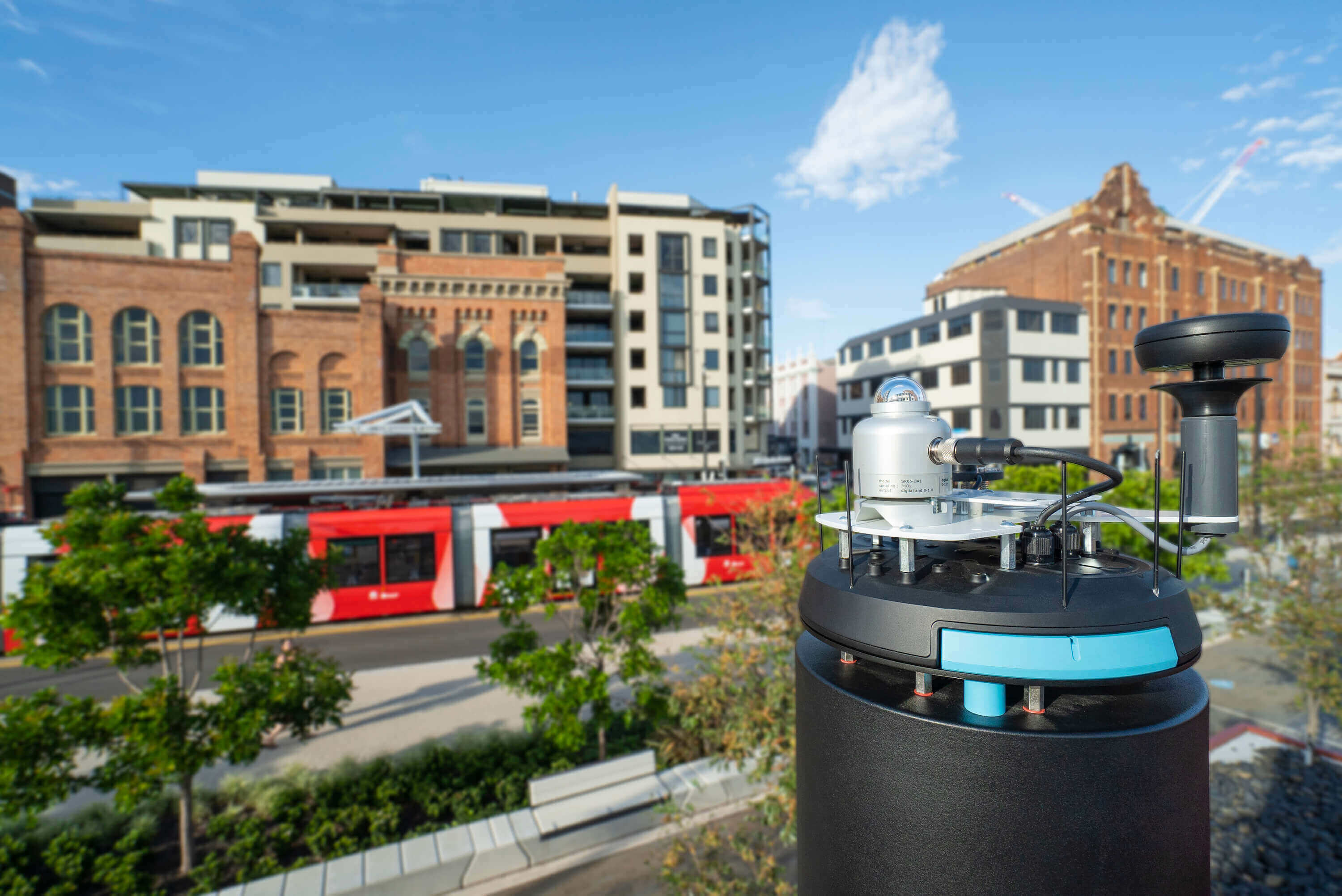
The automated nature of PCB fabrication and assembly services makes it perfect for the mass production of low-cost miniature devices. One such example are smart IoT devices used in smart city applications, whereby thousands of sensors are used to gather environmental data, provide control over infrastructure, and learn from their surroundings. These types of devices often consist of a single PCB meaning that they can mostly be manufactured using a PCB fabrication and assembly service (besides mounting into an enclosure which often uses injection molding).

Automotive modules
The adoption of electronics in modern automotive vehicles has become so great that modern cars are now more electronic than mechanical. In fact, this couldn’t be truer with the introduction of EVs, which rely heavily on power converters, energy storage technologies, and complex computational devices that can monitor conditions around them via cameras in real-time. The complexity of these devices and the need for accuracy makes PCB fabrication and assembly services highly applicable, especially when using services that conform to ISO 9001 and ITAR regulations.

Wearable devices
While the wearable industry is still in its infancy, the numerous technologies offered by modern fabrication services allow wearable devices to take advantage of flexible PCBs, flat cable assemblies, and direct chip-to-board bonding. Such technologies are essential for future wearable devices as wearable devices will only be comfortable if they can move and change shape with the wearer, and this is simply not possible with standard FR4-type PCBs (the most common type in the industry). Flexible PCB technologies also help to reduce fatigue and cracking solder joints which normally occurs when PCBs are exposed to mechanical stresses such as bending, vibration, and impacts.
Why use our service?
With 16+ years of experience, Ponoko is a digital manufacturer that has undertaken all kinds of projects spanning all different industries. This means our engineers not only recognise how to speed up manufacturing times and orchestrate complex projects, but we also understand manufacturing processes and how those processes may affect an engineer's design. As such, our customers are able to fully leverage our experience to ensure the success of their projects while minimizing risk associated with design errors.
Our services are used by numerous industry-leading companies, including Tesla, Intel, Google, and NASA, all of which require the highest standards of quality and precision. In combination with our 365-day guarantee, designers can be assured that electronic assemblies are not only manufactured by an industry-leading software-driven company but can be sure of the longevity of their designs.
PCB fabrication & assembly FAQs
What is a PCB substrate?
What advantages does PCB fabrication and assembly offer?
What are the main types of testing in PCB fabrication and assembly?
Does Ponoko ship worldwide?
How can designers help the PCB assembly process?
Want something else? Check our other services...
PCBA is an essential service for those needing circuit boards, but what about enclosures, mounting brackets, and fittings? Fortunately for engineers, Ponoko offers numerous manufacturing services, including injection molding, laser cutting, and 3D printing, which can be used for both prototyping and production.
For those creating electronic prototypes and need an enclosure, the 3D printing service is by far the best choice thanks to its low entry price and lack of tooling and molds. Those looking to start their first initial production runs, injection molding can be beneficial, especially considering that we offer low-cost prototyping aluminum molds that are much cheaper compared to mainstream stainless steel molds. And for those needing specialized faceplates, our plastic and metal laser cutting service has access to over 200+ engineered materials, allows for order quantities as low as one, and can scale up to tens of thousands.