Schematic Diagram Basics
The process of designing a printed circuit board (PCB) begins with creating a detailed circuit diagram, and this diagram serves as a blueprint for the circuit, outlining each component and its connections, providing a clear roadmap for the PCB design. Understanding the circuit diagram is essential for engineers, as it visually represents the electronic circuit they intend to construct.
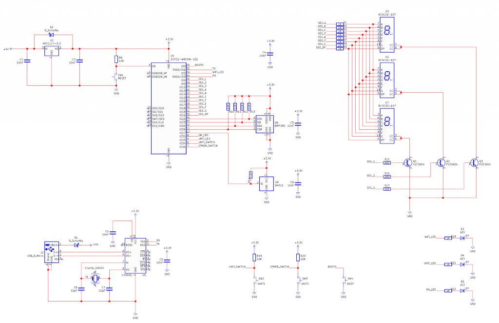
A circuit diagram, also referred to as a schematic, is a crucial tool in electronics engineering as it simplifies complex circuits into standardized symbols and connections, making it easier for engineers to interpret and assemble circuits accurately. These schematics are vital not only during the initial design, but also for troubleshooting and maintenance after the PCB is manufactured. The layout of schematics is generally standardized to enhance clarity and consistency, ensuring that all components and connections are neatly contained within a defined area. This organization is especially important when dealing with complex circuits involving numerous components. Important details, including the name of the designer, affiliated company, revision number, and other pertinent notes, are typically placed at the bottom right corner of the drawing. This information is crucial for maintaining records of the circuit design and ensuring that any modifications or updates are accurately documented.
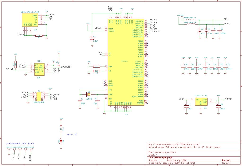
In the past, creating such detailed schematics was a laborious process done by hand. This method was time-consuming and prone to errors, potentially compromising the integrity of the final PCB. However, the introduction of Computer-Aided Design (CAD) tools has revolutionized this process. Today, schematics are drawn electronically using sophisticated CAD software, which has significantly expedited project development by simplifying revisions and enabling more precise drawings.
Modern CAD tools offer advanced features that enhance the design process, including dynamic annotations that update automatically as changes are made and links to datasheets and part numbers that provide immediate access to specifications and supplier information. This integration of resources streamlines the design process, reduces the likelihood of errors, and improves efficiency. The transition from hand-drawn schematics to digitally created diagrams has accelerated the design process while improving accuracy and functionality, showcasing the advancements in electronics engineering.
Standards for Schematic Symbols
For engineers seeking credibility and career advancement, adherence to international standards such as those set by the Institute of Electrical and Electronics Engineers (IEEE) is crucial when drawing schematics. These standards provide a universal language that transcends geographical boundaries, promoting a common understanding among engineers worldwide. The graphical symbols outlined in IEEE standards, such as IEC 60617 and IEEE Std 315-1975, ensure that circuit diagrams and logic functions are easily recognizable and comprehensible.

Interestingly, the standards accommodate regional variations, acknowledging the differences in symbol representation that may seem significant at the national level but are well understood within the engineering community. For instance, the depiction of resistors as either squiggly lines or rectangular boxes is permitted, highlighting the flexibility of standardized symbols.
The importance of standardization also extends to education, simplifying the learning process and ensuring that students acquire the skills and knowledge needed to create accurate technical drawings. The early introduction of standardized symbols and practices in educational institutions equips students with the expertise required to produce clear and concise schematics, paving the way for professional success.
What Are the Different Schematic Symbols?
The world of electronic engineering heavily relies on the use of circuit diagrams or schematics that utilize a wide range of unique symbols to represent various components. While these symbols may vary slightly between different standards such as ANSI and IEC, their use is generally consistent across the industry, allowing engineers to quickly identify and understand the function of each component in a circuit.
A resistor, for example, is represented by a zigzag line with an ‘R’ denoting the resistor, followed by a numeric value representing its resistance in ohms. The use of such a symbol helps engineers recognize the component’s ability to limit current flow, and the value of the resistor indicates its capability to resist current flow.
A capacitor, on the other hand, is denoted with a ‘C’ followed by a numeric value representing its capacitance in farads. The use of two parallel lines with a gap between them also helps engineers recognize the component’s ability to store electrical energy, with the number of lines and the gap representing the component’s ability to store energy and the physical construction of the capacitor.
Inductors, which are critical in controlling energy flow in circuits, are represented with a coil of wire or a series of loops, with an ‘L’ denoting the inductor and a numeric value representing its inductance in henries. The use of such a symbol helps engineers recognize the component’s ability to store magnetic energy, and the value of the inductor indicates its ability to do so.
Integrated circuits and logic devices, which are critical in modern electronics, are represented with a rectangular box and pins that connect to other components. Each pin on the device represents an input, output, or control for the device, with the use of specific symbols on the pin indicating its function. This pin notation helps engineers understand how to use the device, with the position of the pin and the symbol on the pin indicating the state of the output.
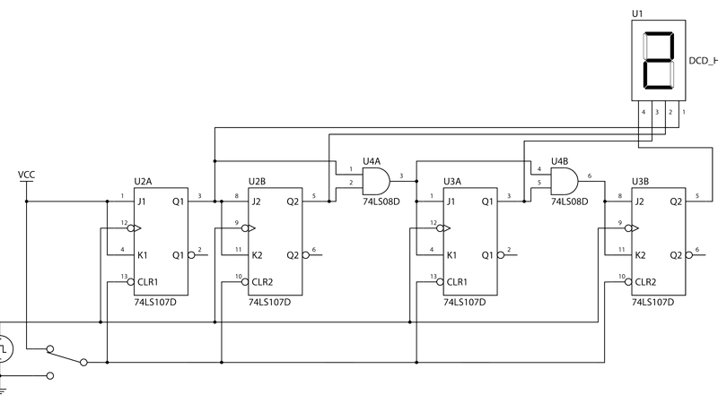
Logic gates, which are the building blocks of digital circuits, also have unique symbols that represent their function. For example, AND gates use a rectangle with a and symbol in the top corner, OR gates use a circle with a + symbol, and NOT gates use a triangle with a in the top corner. This use of a unique symbol for each logic function helps engineers recognize the function of the gate, with the AND gate producing a 1 if all inputs are 1, the OR gate producing a 1 if any input is 1, and the NOT gate inverting the input signal.
Difference Between Schematic & Wiring Diagrams?
While engineers rely on both schematic and wiring diagrams for electrical and electronic systems, these two tools serve distinct purposes and present information in different ways. Schematics focus on illustrating the components of a circuit and their connections, using symbols to represent components and lines to represent connections, which helps engineers understand the functional relationships and operational logic of the circuit without worrying about the physical layout of components. This abstract representation is advantageous when designing new systems, as the resulting diagram helps engineers comprehend how their design will work.
On the other hand, wiring diagrams provide a more literal representation of electrical systems, detailing not only the connections between components but also the physical routes taken by wires between components. This level of detail is essential when installing and maintaining systems, especially in environments where the physical layout of a system is critical to its performance or feasibility, such as buildings and vehicles. A wiring diagram can also be beneficial when troubleshooting electrical systems, as the diagram will show the expected connections and cable paths.
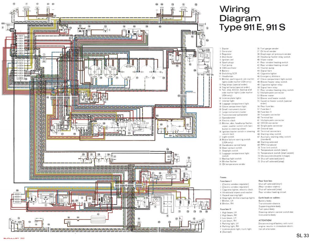
To better understand the difference between these two types of diagrams, consider a central processing unit (CPU). A schematic of such a device would show the logic blocks that process data, including arithmetic logic units, registers, and control units, and how these blocks communicate with each other. However, the physical design of a CPU, where these components are physically located on the chip, would not match the schematic. The schematic ignores the physical layout in favor of showing how the circuit functions, while the physical design shows how the components are wired together on the chip.
A wiring diagram for the same CPU would show the physical connections between components, the type of cable used, and even practical details such as cable thickness and bending radius. This level of detail is essential in high-frequency circuits, where signal attenuation can be a problem, and in power electronics, where safety and efficiency are critical. Such diagrams can also be important in environments where cables and connectors are exposed, such as in automotive systems, where vibration and extreme temperatures can affect cable performance.
How to Read a Schematic
Understanding a schematic diagram is essential for anyone involved with electronics whether it is professionally or as a hobby. A schematic represents electrical connections between components in a circuit using symbols and lines representing wires. The ability to identify components and their connection is vital for building, troubleshooting, and repairing electronic circuits even for those with a basic understanding of electronics. Following a schematic requires adhering to specific rules that simplify the interpretation of the diagram and help users understand the connections and layout effectively.
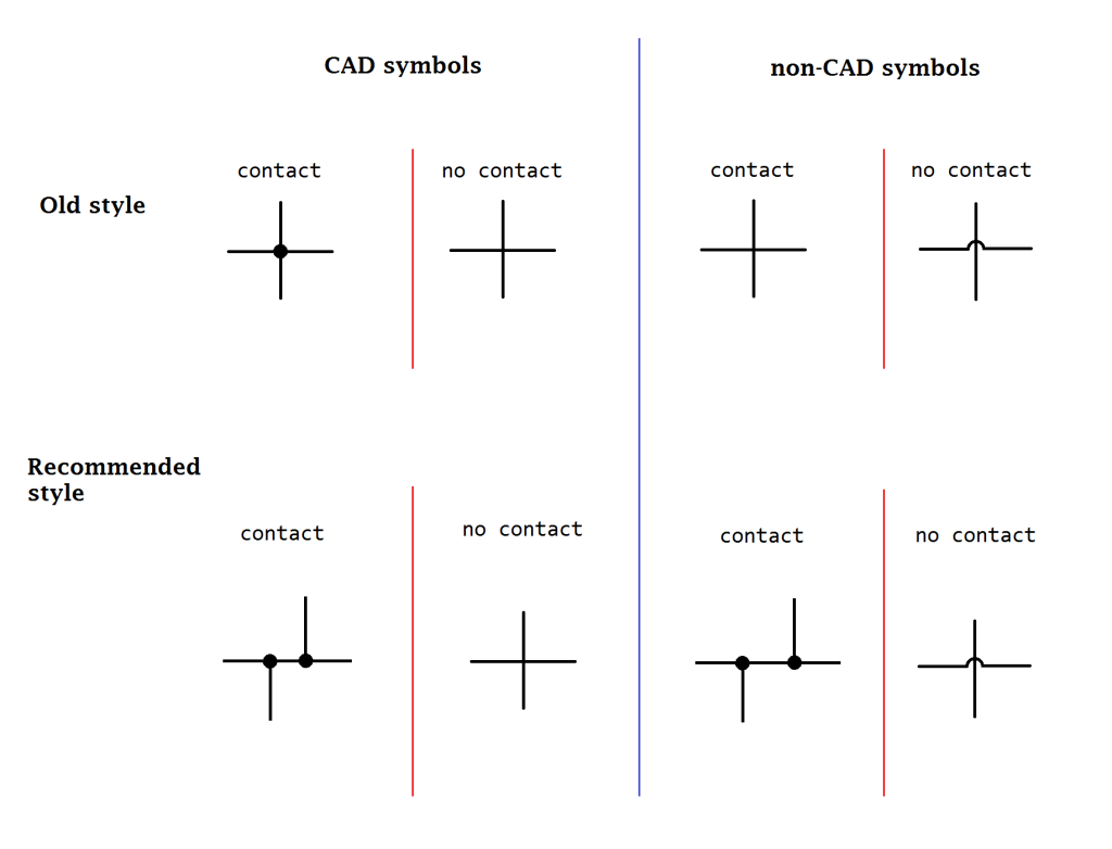
For instance, the representation of connections between wires is crucial as it indicates whether wires are physically connected or not. A dot at a crossing indicates that the wires are connected and allow current flow while the absence of a dot indicates no electrical connection. Misinterpreting these connections can lead to incorrect circuit assembly or troubleshooting potentially causing circuit failure or damage to components.
The connection of wires to components on a schematic also plays a key role. Any wire leading into a symbol is connected to that component and enables electrical flow to and from components. Understanding this connection helps users comprehend how current flows through the circuit and how components interact with each other.
The labeling of components on a schematic directly correlates to their identification on the physical circuit board or PCB. Components on a schematic are labeled with unique identifiers such as R1 for the first resistor and C1 for the first capacitor. This labeling convention helps users easily locate and identify components on both the schematic and PCB. Misinterpreting these labels can lead to incorrect component placement on the PCB and is essential to correctly assembling electronic devices.
How Do You Create a Schematic Diagram?
The use of Computer-Aided Design (CAD) software has become essential for creating detailed and precise drawings intended for manufacturing and professional review. Unlike traditional hand-drawn methods, CAD software offers a multitude of advantages, including the ability to share and edit designs digitally, incorporate real-time data and simulations, and integrate back-annotation with printed circuit board (PCB) designs. A CAD tool that also supports PCB design ensures a seamless transition from schematic to PCB layout, reducing the likelihood of errors and speeding up the design process.
While both open-source and paid solutions are available for schematic and PCB design, KiCad stands out for its cost-effectiveness and flexibility. As an open-source package, KiCad offers customization options and community support, making it a popular choice among engineers. However, professional tools like Eagle and Altium also have their own advantages, including advanced features and reliable performance. These tools are favored by professionals for their ability to handle high-speed PCB design and intricate layout routing.
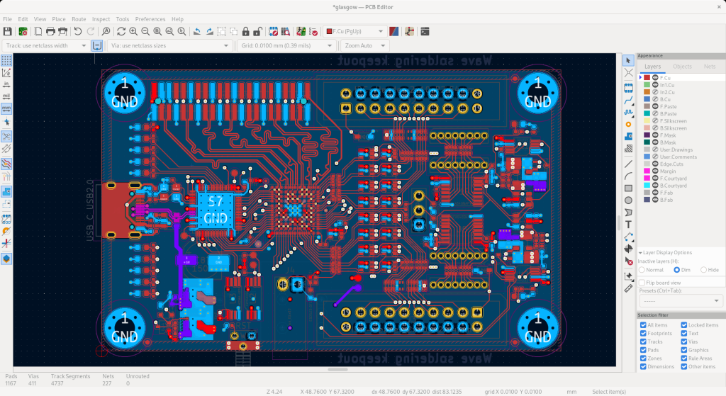
The integration of CAD tools with PCB design capabilities has revolutionized the way engineers develop and collaborate on projects. The ability to create and edit designs digitally enables engineers to work efficiently and effectively, while the integration of simulations and real-time data helps to improve the accuracy and reliability of designs. The future of CAD and PCB design will likely involve more advanced features and capabilities, such as AI-assisted design and virtual reality prototypes.
Rules for Drawing Schematic Diagrams
In engineering, particularly when dealing with electrical schematics and circuit designs, adherence to standard practices is crucial for ensuring clarity, efficiency, and safety. Engineers are encouraged to use universally recognized symbols and wiring conventions to promote uniformity in design documentation. This approach minimizes errors and facilitates easier maintenance and troubleshooting by other professionals who may interact with the diagrams.
The inclusion of all components in schematics is another critical practice. This ensures that every part of the circuit is accounted for, aiding in comprehensive understanding and accurate assembly or analysis of the system. For instance, if a schematic includes all variants of resistors, capacitors, and other elements, it becomes straightforward for anyone reviewing the diagram to understand the complete functionality and requirements of the circuit.
Legibility is another key aspect of effective schematic design. Utilizing clear, readable text is essential, as this allows individuals analyzing the diagram to easily identify each component and understand its purpose. The use of monospaced fonts is a common practice in this regard, as these fonts help maintain uniformity and spacing in the text, making it easier to read and less prone to misinterpretation.
Standardized references and annotations are also highly beneficial. Labeling components with universally accepted abbreviations, such as R for resistors and C for capacitors, aligns with industry standards and enhances the readability of schematics. This practice not only helps reduce the learning curve for new engineers but also ensures that experienced professionals can quickly interpret and work with the diagrams without confusion.
Spatial arrangement in circuit diagrams is equally important. By spacing out the components adequately, engineers can avoid clutter that might obscure important details of the circuit. A well-organized layout helps in identifying the relationships and connections between different components, thereby reducing the risk of errors during the building or testing phases.
Finally, avoiding crossed wires in diagrams unless absolutely necessary is crucial. Crossed wires can often give the misleading impression that they are electrically connected, leading to potential misinterpretation and error in circuit construction or analysis. In cases where crossing wires is unavoidable, differentiating techniques such as jumps can be used to visually indicate that wires do not connect.
Key Takeaways
Schematic diagrams are a crucial component in the world of electronics as they provide a visual representation of electrical circuits. Unlike architectural or engineering drawings, schematic diagrams do not concern themselves with the physical dimensions or precise placement of components but instead focus on illustrating the electrical relationship between components. The use of lines represents wires, and standardized symbols represent components, allowing anyone involved with electronic design to understand the function and operation of the circuit.
The use of standardized symbols is essential for clear communication and is vital in the global electronics industry. Each symbol corresponds to a specific component, and these symbols are universally recognized. This means that a schematic designed in one country can be used for manufacturing in another without the need for changes. If symbols were not standardized, then designs would need to be altered for each country or region, and this could lead to errors during manufacturing and use.
CAD software has become the norm in the field of engineering and is essential for creating schematic diagrams and designing PCBs. Programs such as KiCad allow engineers and designers to create detailed schematics that can then be directly used for PCB design. These tools also provide libraries of standard symbols and components that help to ensure designs conform to engineering and industry standards. Furthermore, many CAD tools can check a design for errors, ensuring that circuits operate as expected.
Once a schematic has been designed using CAD, the next step is to create a PCB based on the schematic. This involves deciding where components will be located on the PCB and routing wires between components. The ability to complete this step in the same software environment as the schematic helps to ensure that the PCB is designed correctly and that the schematic and PCB match.
In essence, schematic diagrams help engineers understand how components fit together to produce a functioning circuit. By using standardized symbols and advanced CAD tools, these diagrams aid in the design, manufacturing, and use of electronic devices, ensuring that devices operate as expected and that engineers can easily maintain and repair circuits. The importance of schematic diagrams cannot be understated, and their role in the field of electronics will only continue to grow.
