What’s a PCB?
A Printed Circuit Board, or PCB, is a substrate that connects electronic components together, and has been a critical technology in the field of electronics due to its ability to simplify the construction process of circuits, while enabling extremely advanced technologies.
The design of a PCB is a meticulous process that requires skilled engineers to map out the placement of components based on the electrical requirements of the device. Each PCB is customized to ensure efficient manufacturing and optimisation, especially when considering that modern electronics applications demand highly specialized and miniaturized devices.
The manufacturing of PCBs utilizes printing techniques, such as lithography and screen printing, which not only makes mass production feasible but also affordable. This affordability has been a key factor in the widespread adoption of PCBs, allowing for electronics to be integrated into a wide range of industries, including healthcare, automotive, consumer electronics, and aerospace.
Without PCBs, electronic components would have to be manually wired together, requiring laborious and precise soldering. Such an approach almost always leads to errors and inconsistencies, compromising the functionality and reliability of devices. Furthermore, manual wiring is impractical for modern electronics, which require extremely small components that cannot be easily manipulated due to their size.
The precision offered by PCBs has also enabled the development of incredibly small electronic components, with some traces being thinner than human hair. This precision allows for powerful components to be integrated into tiny spaces, something which would otherwise be impossible.
Composition
At the heart of a PCB is the core material, commonly referred to as the substrate. This foundational layer acts as the physical base upon which all other components are mounted. Typically made from a type of fiberglass known as FR4, the substrate is chosen for its electrical insulation properties, ensuring that no unwanted electrical currents flow between the different layers of the board. This insulation is critical for the stable and safe operation of the electronic device.
In more specialized applications, such as high-frequency electronics found in aerospace or advanced telecommunications, the core layers may be crafted from high-grade ceramics. These materials are selected for their ability to provide extremely well-controlled impedances, which is essential for maintaining signal integrity in environments where even minor disruptions can lead to significant performance issues or data loss.
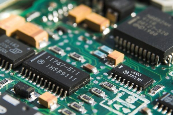
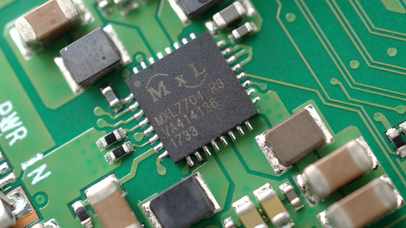
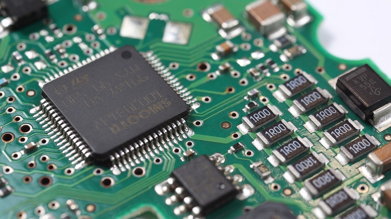
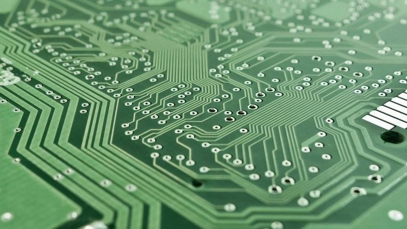
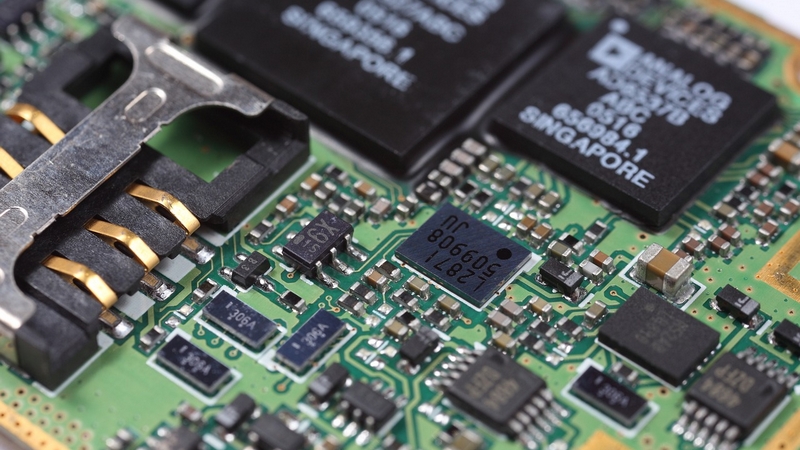
Surrounding the core material are multiple layers of copper, which are crucial for the conduction of electricity throughout the PCB. These copper layers are meticulously arranged, with each layer being sandwiched between the substrate layers. The arrangement is crucial as it defines the path that electrical currents will follow across the board. Notably, the outermost layers of copper are exposed, allowing for connections to other components like resistors, capacitors, and integrated circuits.
To establish connectivity between these copper layers, manufacturers drill holes through the PCB, known as vias. These vias are then plated with copper to create a conductive tunnel that links multiple layers of the board, facilitating complex and multi-layered circuit designs that can perform a wide array of functions within a relatively small footprint.
Protecting these critical copper traces is the role of the solder mask layer. This layer is applied over the copper traces and vias, safeguarding them against oxidation and corrosion, which could otherwise compromise the board’s functionality. Additionally, the solder mask helps prevent electrical shorts during the soldering process by providing a barrier that keeps the solder from bridging unintended gaps between circuit paths. Traditionally, this layer imparts PCBs with their characteristic green color, although other colors such as blue, red, or black can also be used depending on the manufacturer or specific application requirements.
Finally, the silkscreen layer is applied. This topmost layer contains all text and graphics that are visible on the PCB, including component designations and general information about the circuit board. The silkscreen layer also helps with component identification during the manufacturing and repair processes and can be useful for debugging electrical issues.
The combination of all these layers enables the creation of highly advanced circuits that are reliable and easy to manufacture. The resulting product is a precision-engineered component that is ready for use in a wide range of applications, from consumer electronics to medical devices to military systems. The end result is a real-life puzzle, one that only a few can truly appreciate—the effort and complexity that goes into the manufacture of a modern printed circuit board.
Types of Printed Circuit Boards
The electronics industry is dependent on the development of various PCB technologies to enable the creation of complex circuits. Among the many types of PCBs available, each type is specialized to cater to specific applications and is a function of the number of copper layers on the PCB.
The simplest PCBs are single-sided and consist of a single layer of copper foil laminated onto a non-conductive substrate. Components are mounted on one side, and copper traces on the other side connect these components together. Their simplicity also means that they are the cheapest PCB option and are typically used in simple electronics such as power supplies and sensors. However, their simplicity also introduces several limitations. For example, the absence of a second layer means that ground pours are not possible, and this limits the ability to reduce noise in circuits. Additionally, the inability to have plated-through holes also limits the maximum complexity of a design.
Double-sided PCBs are the next level of complexity and feature copper layers on both sides of the substrate. This allows for double-sided PCBs to have plated-through holes, and this enables them to support more complex designs. The use of plated-through holes also means that signals can be taken from one side of the PCB to the other without needing additional components or traces. As such, double-sided PCBs are ideal for applications that require a good balance between design complexity and cost. They are commonly found in industrial control equipment and consumer electronics where design density is moderate.
Multi-layer PCBs are the most advanced PCB technology and consist of three or more copper layers that are sandwiched with insulating layers. The use of additional copper layers allows for significantly higher design densities, and the ability to have power and signal planes helps to improve signal integrity. The high-speed capabilities of multi-layer PCBs make them ideal for high-speed and high-frequency applications such as computer networking equipment, smartphones, and other advanced electronic devices. While these PCBs are the most expensive option, their ability to support thousands of connections and manage issues related to electromagnetic interference and heat dissipation makes them a cost-effective option for complex devices.
Finally, flex PCBs are highly specialized PCBs that are designed to be flexible and are commonly found in wearable electronics. These PCBs are often constructed with Teflon and can bend and twist without damaging their circuitry. As such, they are ideal for applications that require a PCB to conform to a particular shape or surface and are also ideal for applications with dynamic connections.
Terminology to Know
In the intricate world of PCB design, understanding the specific lingo and terminology is imperative for both newcomers and seasoned engineers. Each term encapsulates a vital aspect of the PCB’s structure and functionality, influencing everything from manufacturability to performance.
One of the most pivotal terms in PCB design is the “layer count,” which refers to the number of copper conductive layers in the PCB. These layers are central to the PCB’s operation as they facilitate the flow of electrical signals between various components. The layer count can vary substantially, from simple two-layer boards commonly found in household electronics, to complex, multi-layer boards used in advanced communication devices or computing hardware. More layers enable for more complex and dense circuit configurations, accommodating more functions in smaller spaces.
An additional key term is “minimum trace width.” This defines the narrowest width that a conductive track can be manufactured on the PCB. Trace widths are pivotal because they determine how much current can safely pass through the circuit without overheating and potentially damaging the board. In high-density applications like modern microprocessors, traces can be only a few micrometers wide, allowing for a greater density of circuits within a given area.
Closely related to trace width is “minimum clearance,” which specifies the smallest allowable distance between any two conductive elements, such as traces or pads. This spacing is essential to prevent electrical shorts and ensure the reliability of the PCB. In environments where electrical interference or high voltages are a concern, greater clearances might be necessary to avoid cross-talk between circuits or potential arcing.
The term “copper weight” refers to the thickness of the copper layers on the PCB, typically measured in ounces per square foot. The weight directly influences the current-carrying capacity and thermal characteristics of the PCB. For example, a 1-ounce copper layer translates to approximately 35 micrometers (um) in thickness. Thicker copper layers can carry more current and are preferable in high-power applications, but they also contribute to the overall weight and cost of the PCB.
Finally, “PCB thickness” describes the overall thickness of the entire board, which affects both the mechanical stability of the board and how it fits into a device assembly. Common thicknesses include 1.6mm, which provides a good balance between strength and flexibility, and 0.8mm, often used in smaller, lighter devices. The choice of PCB thickness impacts not just the physical attributes of the PCB but also its performance and manufacturing process.
How to Design Your Own PCB
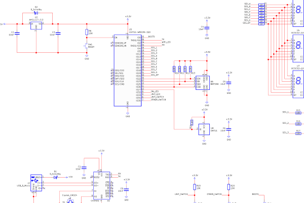
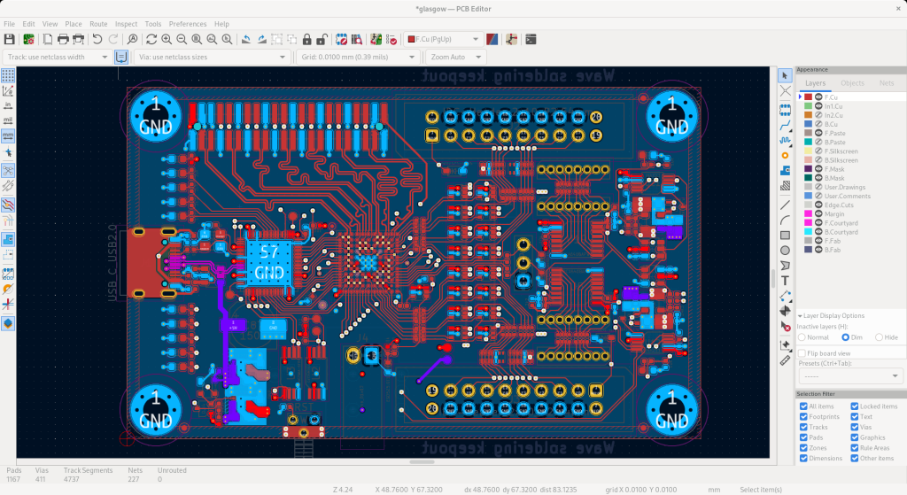
Designing printed circuit boards has become more accessible thanks to the advancement of electronic computer aided design software. These tools allow both amateurs and professionals to design complex electronic circuits with precision and efficiency. Of the many tools available, Altium Designer and Eagle stand out as industry standards offering robust features that cater to intricate design requirements including multi layer boards and precise routing capabilities. However, the downside is that they are paid programs requiring users to purchase licenses which can be a barrier for individuals or small companies with limited budgets.
Learning these tools is a valuable investment as mastery of Altium or Eagle can significantly enhance employability in the electronics industry. These skills are highly sought after as they directly apply to a wide range of engineering tasks from simple gadgets to complex multi functional devices. The ability to proficiently use such software can open doors to career opportunities in electronics design and manufacturing.
For those seeking a cost effective alternative KiCad presents a compelling option. As an open source software it is completely free making it accessible to anyone regardless of budget constraints. KiCad has gained popularity for its powerful features that rival those of its paid counterparts. It supports a wide range of functionalities needed for professional PCB design including schematic capture PCB layout and 3D viewing of the assembled board. Its capability to run on multiple operating systems including Windows Mac and Linux further enhances its versatility ensuring that it can be used on virtually any computer.
KiCad’s adaptability extends to its support for custom plugins and the ability to import and export files in various formats. This flexibility makes it an excellent tool for collaboration and integration with other software solutions streamlining the design process and facilitating a more efficient workflow. The growing recognition of KiCad’s capabilities is evident as notable tech companies including Raspberry Pi and Arduino have begun to adopt it for their development projects signaling a shift in the industry towards more open source solutions.
For those looking to hone their skills in PCB design software YouTube serves as an invaluable resource. The platform offers countless tutorials and how-to videos that cover everything from basic introductions to advanced techniques. These resources are particularly useful for self learners and provide a practical way to improve one’s proficiency in using these complex tools whether one opts for a professional paid tool like Altium a free solution like KiCad or anything in between the wealth of resources available makes it easy to gain expertise in PCB design software.
The integration of open source solutions like KiCad into large companies also demonstrates the power of open source software. The ability to collaborate with engineers from all backgrounds and industries can accelerate the development of projects and products. The use of open source tools also promotes transparency and accountability through public access to designs and code. This can be particularly beneficial for projects with a focus on security and privacy such as internet connected devices.
As the demand for professional PCB design tools increases so does the competition in the market. Companies that can provide innovative and cost effective solutions will gain a competitive edge. The development of new features and functionalities will continue to enhance the capabilities of PCB design software. The shift towards open source solutions also indicates a move towards increased collaboration and sharing of knowledge in the electronics industry.
The future of PCB design software holds promise with the integration of advanced technologies such as AI and machine learning. These tools can automate repetitive tasks, enhance productivity and improve the accuracy of design files. The integration of these technologies also indicates a move towards increased standardization in design files and the use of industry approved formats.
Key Takeaways
Printed Circuit Boards, or PCBs, are fundamental components in the world of electronics acting as the backbone for virtually all electronic devices. These boards are meticulously designed to connect various electronic components through a network of copper pathways also referred to as traces. These traces facilitate the flow of electrical signals and power throughout the device enabling it to perform its designated functions. From smartphones and computers to more complex systems like automotive electronics and satellites PCBs are integral in providing the necessary connectivity and functionality.
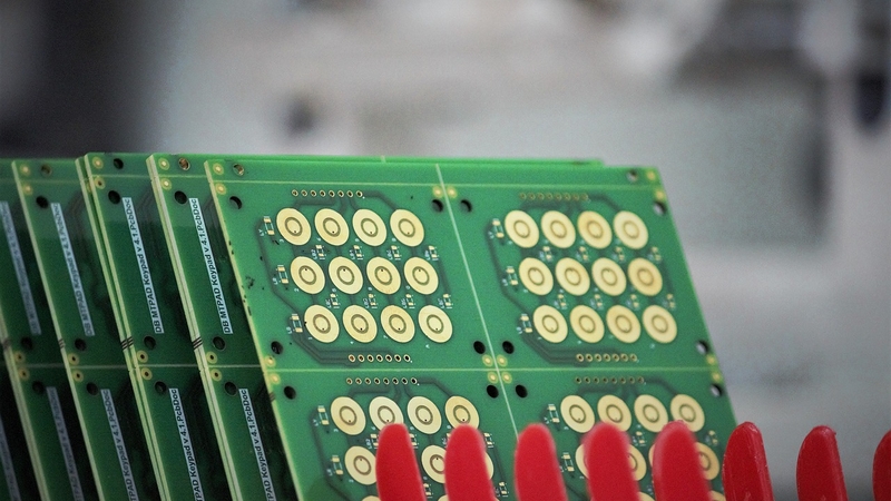
The production of PCBs has become highly efficient allowing them to be manufactured in large quantities while maintaining precision and reliability. This scalability is crucial in meeting the global demand for electronic devices. Modern manufacturing techniques such as automated assembly lines and surface mount technology have streamlined the production process. These advancements not only enhance the production speed but also significantly reduce the occurrence of errors ensuring that each PCB meets the stringent requirements of today’s technology.
Despite the complexity of their design and function the terminology surrounding PCBs is surprisingly straightforward. Terms such as traces, pads, layers and vias are commonly used to describe the various aspects of PCB design and function. For instance traces refer to the copper pathways pads refer to the contact points where components are attached layers denote the levels of copper and insulating material in a PCB and vias refer to the holes that allow connections between different layers. Understanding this lingo is essential for anyone involved in electronics design or manufacturing as it facilitates clear communication and enhances the efficiency of the development process.
Designing PCBs has become more accessible than ever thanks to a wide range of software tools available to both professionals and hobbyists. These tools range from high-end paid programs that offer extensive features and support for complex projects to free software that is perfect for beginners or smaller projects. Paid tools often provide advanced capabilities such as auto-routing simulation and 3D modeling which are invaluable for intricate and multi-layer designs. On the other hand free tools while sometimes limited in features still offer the essential functionalities required for designing functional PCBs. They provide a great starting point for those new to electronics design allowing them to learn and experiment without significant investment.
In conclusion PCBs are a cornerstone of modern electronic design providing the critical connections needed for devices to function. Their ability to be produced at scale ensures that the ever-growing demand for electronic devices can be met efficiently.
Why Choose Ponoko
The process of manufacturing a printed circuit board is a complex and time-consuming task that requires meticulous attention to detail, taking away from engineers’ primary focus on innovation and design. The need to source components and find reliable manufacturers adds to the challenges faced by engineers, with the quality of the final product having a direct impact on the functionality of the device.
While engineers can handle these logistical tasks, the time spent on component sourcing and manufacturer liaison takes away from the value they bring to a project, potentially leading to preoccupation with operational details such as production issues and quality control.
Ponoko offer engineers a solution to this manufacturing challenge, taking over the production responsibilities to allow engineers to focus on design and innovation. With years of experience in manufacturing and a precision part rate of 99.7%, Ponoko is able to deliver high-quality parts and PCBs that meet the exact specifications, ensuring reliability and consistency.
Ponoko’s ability to outsource the manufacturing process from engineers also enables accelerated project timelines, reducing costs and enhancing product quality. Thus, this partnership enables engineering teams to focus on advancements and innovations across various technology sectors, ultimately leading to groundbreaking technological progress. The reliance on a single source for both prototyping and mass production helps to standardize the design and manufacturing process, reducing the complexities involved.
Overall, Ponoko’s specialized services enable engineers to maximize their productivity and focus on what they do best, while ensuring the quality and reliability of the final product.
FAQs
- What is a PCB?
- A printed circuit board, or PCB, is a fundamental part of modern electronic devices and ensures that various components such as capacitors, resistors, and integrated circuits work in unison to perform their designated functions. The substrate of a PCB is made from fiberglass, specifically FR-4, which provides a sturdy yet flexible base, and the conductive connections are made of copper due to its excellent electrical conductivity. To prevent accidental electrical shorts, a solder mask, which is typically green, is applied over the copper, and a silkscreen layer is applied on top for labels and component indicators that aid in the assembly and maintenance of the board.
- What are the main components of a PCB?
- The main components of a PCB include pads, traces, vias, and planes. Pads are the small surface areas coated with tin-lead or gold over nickel where components are soldered onto the PCB, traces are thin lines of copper that connect pads to each other ensuring electrical flow between components, vias are holes in the PCB that allow connection between different traces, and planes are large areas of copper that act as power supply or ground providing a stable voltage level across components.
- How are PCBs designed?
- Designing a PCB is a complex process that starts with schematic capture where the circuit layout is initially drawn using specialized software. This is followed by the board design where the physical layout of the PCB is planned including the placement of components and routing of electrical connections. Advanced software tools allow designers to simulate the behavior of the circuit to identify potential issues before the board is manufactured.
- How are PCBs made?
- The manufacturing process of PCBs involves several steps including the printing of the design onto a laminate board, etching of the copper to reveal the design, drilling of holes for vias, coating to protect the copper from oxidation and to insulate traces, and the final soldering of components either by hand for prototypes or by automated machines for mass production.
- What types of PCB exist?
- There are various types of PCBs each suited to different applications with single-sided PCBs having components on one side and are used in simple electronics, double-sided PCBs having components on both sides, and multi-layer PCBs that can have up to 10 layers separating traces from each other.