Our Process for Rapid PCB Manufacturing
When starting a new project, engineers have so much to consider, from the core functionality of their circuit all the way to the manufacturing and distribution. Of course, the heart of any project is the design itself, but the supporting cast of characters, such as component selection and PCB layout, play just as an important role.
The thrill of seeing a design come together can quickly give way to the stress of manufacturing if engineers are not careful. For example, a component that is currently in stock may have a discontinued notice from its manufacturer, or a part that is on backorder could see a delay in the manufacturing process. Such issues can also arise from using generic part numbers that cover a range of different parts, with the result being a component that is not suitable for an application.
Trying to catch these problems before they manifest during manufacture can also be problematic, to say the least. Engineers need to be able to anticipate how their design will be manufactured, and this requires experience in the field which not all engineers have.
This is particularly a challenge for engineers who are using rapid prototyping stages before committing to mass production. Such stages are essential in testing a design for performance and functionality, but making mistakes at this stage can be costly.
But don’t worry, our rapid prototyping and manufacturing services have been designed with engineers in mind. Our software-powered tools recognise potential problems before they manifest, ensuring that the few minutes spent on checking a design are used efficiently.
Once a problem is identified, our engineers will not only help find a solution but also ensure that the solution is implemented into all designs currently in the prototyping and manufacturing stages. The result is a rapid response to any unforeseen challenges that can cost engineers both time and money.
By leaving the manufacturing and prototyping stages to us, you can focus on the aspects of a project that are interesting, whether that is exploring new technologies, designing new products, or solving difficult problems. The use of our rapid prototyping and manufacturing services means that the circuit design stage is the only stage that engineers need to focus on.
Benefits of Quick Turnaround
When designing a product, time is everything, and the faster a prototype can be manufactured and tested, the better. The quicker a prototype can be spun, the sooner it can get into the real-world where it can be subjected to all manner of different conditions, used by real people, and then checked for performance. As such, engineers can quickly identify issues with their design, and this allows for fundamental changes to be made before the product enters mass production.
The importance of time in the prototyping stage also means that engineers spend less time stuck in laboratory conditions, using equipment, and conducting experiments. The faster that a prototype can be developed and tested, the more time there is for other essential tasks, such as drawing up plans for the next prototype, researching new ideas, and making alterations.
Furthermore, the ability to rapidly produce prototypes also allows engineers to stay ahead of the competition. A design that reaches the market before its competitors not only helps to establish a product as a market leader, but also provides a barrier against copycats wanting to capitalize on the original design. The quickness with which a prototype can be developed also allows for market research to be done faster, which helps engineers understand how their product will be received as well as identify potential problems before they manifest in the real-world.
Finally, the ability to rapidly create prototypes also helps engineers by enabling them to make multiple design iterations in a short period of time. With each prototype, engineers can identify areas that need improvement, make alterations, and then roll out new designs. This rapid cycle of design, test, and change helps to accelerate the product development process, resulting in less time spent on development and thus, reducing the cost of development.
Overall, creating a prototype is one of the most important steps in the engineering process, and the faster a prototype can be manufactured and tested, the better. By spending less time on prototyping and more time on other essential activities, engineers can accelerate their time to market, outmanoeuvre competitors, and improve their products.
How it Works (Step-by-Step)
When a PCB is designed, it is essential that engineers not only get the layout of their design correct, but also create a bill of materials (BOM) that lists all the components needed for that design. Just like how a shopping list helps when going to the grocery store, a BOM helps manufacturers know exactly which parts to source before they can begin manufacturing. Thus, the first crucial step after a PCB is fabricated is to generate a BOM which describes each component used on the PCB, including its quantity, description, and reference number.
Once a BOM has been derived from a PCB design, the next step for engineers is to submit their design to a manufacturing house for further processing. At this stage, our in-house software tools will then check a design for errors that may not be obvious to engineers, including trace issues, cutouts, and drill sizes. These checks help to prevent costly mistakes during the manufacturing process, thereby reducing the time taken to deliver completed PCBs to engineers.
After a design has been checked for manufacturing errors, our specialists will then take all the needed manufacturing files and source the parts needed for that design. This means that engineers do not need to worry about sourcing components or organizing parts; all of this is handled by our team. Finally, we can then begin manufacturing the PCBs, and these are shipped directly to engineers for testing and deployment.
Key Takeaways
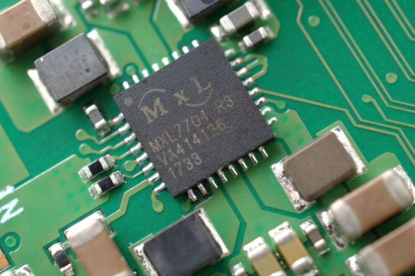
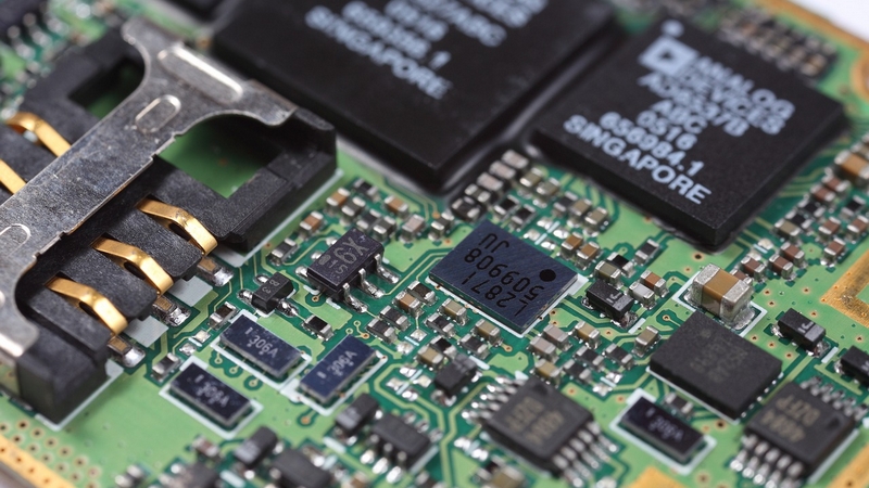
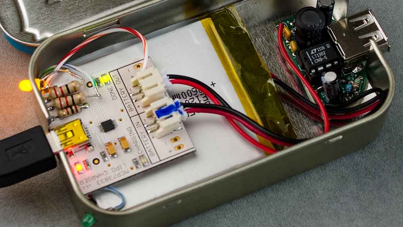
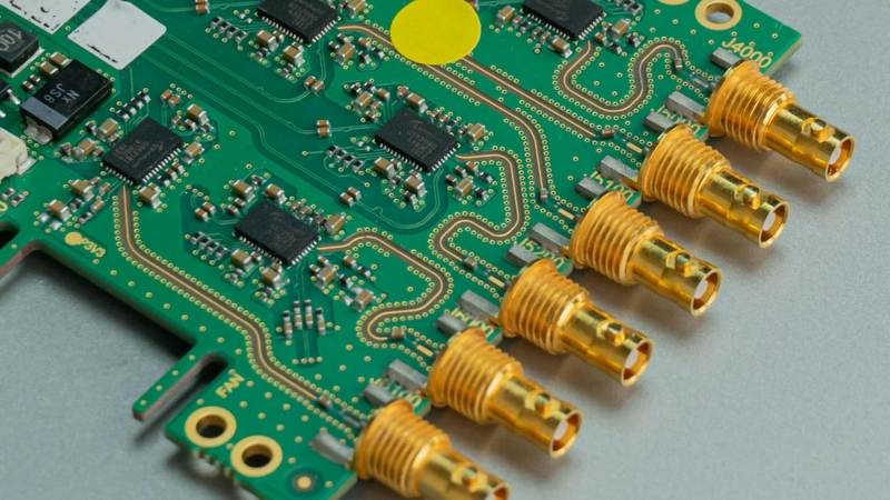
When rushing to get prototypes out into the world, it is essential that all aspects of a prototype are given proper attention, especially when it comes to the foundation of that prototype, the PCB. PCBs are extremely effective at simplifying circuitry, increasing signal integrity, and even aiding in component selection (as many components can only be soldered to PCBs), but their complex nature means that even the most skilled engineers can struggle with their manufacture and configuration.
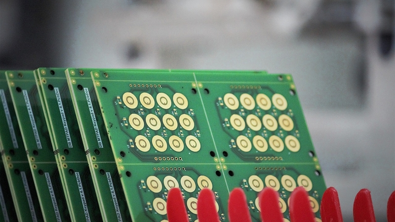
The first major hurdle that engineers can face is getting their PCBs fabricated with no errors. Even the most basic 2-layer PCB can have a multitude of manufacturing and design challenges, such as trace widths, space constraints, and layer alignment, meaning that a single mistake in the design file can result in an entire production run being scrapped. At the same time, these challenges can also lead to manufacturing issues, such as rough edges and poor solderability, which will make that prototype unreliable in the long run.
The component side of PCBs also presents engineers with a range of issues, including component sourcing and compatibility. For example, some components may be unavailable from distributors, or may require specific variants (such as temperature range), meaning that an entire PCB design is dependent on parts that may not exist.
As such, it is clear that PCBs are far from trivial to manufacture, with a multitude of interdependent factors that need to be considered. Thankfully, our experts have decades of experience in the field of PCBs and can take away the stress of getting PCBs fabricated and assembled, allowing engineers to focus on the aspects of their prototypes that will set them apart. By using our services, engineers can rest assured that their PCBs will be manufactured by experts who not only understand the ins and outs of PCB manufacturing, but also have access to a wide range of resources and industry contacts that ensure rapid prototyping, component sourcing, and manufacturing.
The result of our services is that engineers can get PCBs made at speed, without having to worry about the many challenges that they can face. With our help, engineers can reduce their time to market, accelerate their development cycles, and get back to focusing on what makes their prototypes special.
Why Choose Ponoko
When it comes to prototype manufacturing and subsequent initial production runs, Ponoko has been at the forefront of the industry for over 15 years, having been responsible for more than 2 million parts used across all areas of engineering. Whether it is the extreme conditions at the bottom of the ocean or the harsh environment of space, Ponoko parts have been utilized in a wide range of different applications, demonstrating Ponoko’s ability to produce precision parts no matter where they are used.
As Ponoko has such extensive experience in the engineering field, Ponoko fully understands the importance of both precision and quality, but also the need to accelerate project development. For example, complex prototypes typically take a long time to produce, and this can be problematic for projects that have tight deadlines. Recognising this challenge, Ponoko is constantly developing new manufacturing services, as well as tools that can help accelerate projects, so that prototypes can be produced faster, and thus, help to expedite development times.
Finally, Ponoko is also dedicated to providing innovations in both prototyping and initial manufacturing stages. For instance, Ponoko is at the forefront of digital manufacturing, having developed digital tools that can help speed up project development by eliminating the need for manual design validation. By combining digital technologies with traditional manufacturing processes, Ponoko is able to offer engineers with the latest prototyping technologies, ensuring that the most advanced concepts can be realized.