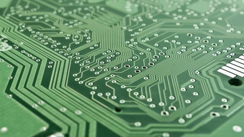
What is a PCB?
The invention of the Printed Circuit Board, or PCB, has revolutionized the world of electronics, providing engineers with a practical method for creating complex circuits. Instead of using large bulky wiring schemes, a PCB allows for thousands of connections to be made in a very small space, resulting in a significant reduction in size. This reduction in size also makes PCBs highly practical in portable electronics, such as laptops and smartphones, which could otherwise be as large as desktop computers.
The use of a PCB also significantly reduces the labor costs associated with creating electronic circuits. The photographic imaging process used to apply copper wires to a substrate makes mass production extremely economical, even at small scales. This is also advantageous for prototypes, which can be produced in small numbers and provide engineers with a physical device to test and modify.
The high degree of accuracy offered by PCB manufacturing also makes PCBs ideal for advanced electronic circuits, such as those used in defense, medical and aerospace applications. The narrow trace widths and precision soldering enable high-speed data transfer and precise control, something which is essential for modern computing and communication systems.
Overall, the PCB has become the foundation of modern electronics, providing engineers with a practical, economical and accurate method for creating circuits. From humble beginnings to desktop processors and advanced RF systems, the PCB has played a critical role in the development of electronics as we know it.
What is PCBA?
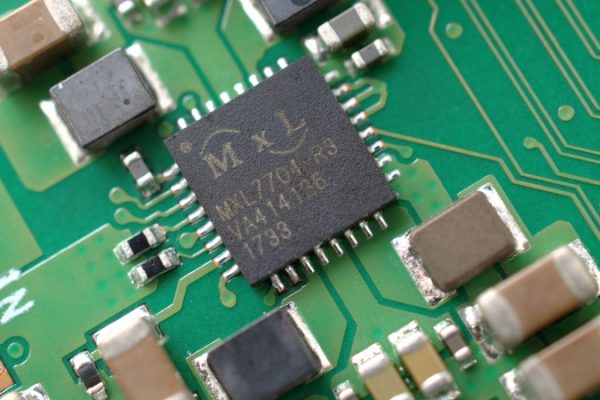
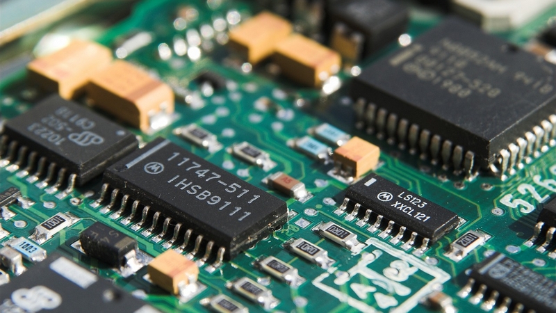
Printed Circuit Board Assembly, or PCBA, is the manufacturing process that takes components and places them onto PCBs to make a complete circuit. This process was historically manual, when through hole components dominated the industry (this is where component leads are placed through holes in a PCB).
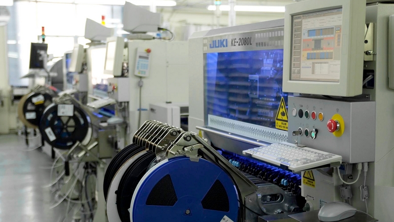
However, the development of SMD parts has allowed for pick and place machines to automatically place components onto PCBs, greatly speeding up the speed of PCB assembly in both prototypes and production parts. This rapid population also allows for designs to be tested sooner, thereby aiding product development cycles.
PCBA is also advantageous as it is able to insert SMD parts with great precision. These components are notoriously difficult to hand solder, and their small size means that trying to place them manually is also difficult. Instead, PCBA uses pick and place machines that position components onto PCBs with great repeatability, and this precision also makes PCBA ideal for soldering.
Another major benefit to using PCBA is that it is an extremely cost-effective process. The ability of PCBA to rapidly produce circuits along with the many thousands of circuits that can be produced on standard PCB assembly lines means that the cost per circuit is extremely competitive. This is also advantageous for prototyping as the cost to prototype a circuit is far lower than one would expect.
However, it is important to note that PCBA does not include the manufacturing stages of a PCB such as image etching and copper plating. These stages are performed before the PCB is sent to a PCBA service, and these stages are also essential for the proper functioning of a PCB.
Overall, PCBA provides engineers with an extremely rapid, cost-effective, and precise manufacturing and prototyping service that is ideal for getting PCBs populated with components.
Comparing the Printed Circuit Board processes
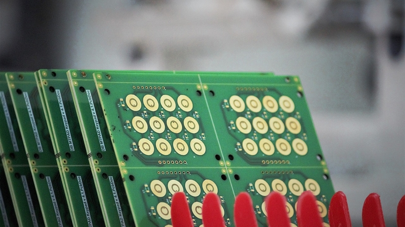
The process of manufacturing printed circuit boards (PCBs) is a remarkable feat of engineering, requiring a high degree of precision and attention to detail. To start, the bulk of PCBs are manufactured using a layered approach, with multiple copper clad boards stacked on top of each other. This layered construction allows for extremely complex circuits to be made, with as many as 32 copper layers being possible.
The first stage of PCB manufacturing involves drilling, where all the boards (both individual and stacked), are drilled simultaneously to create holes for components, wires, and vias.
After drilling, PCBs then move on to chemical etching, where unneeded copper is removed from the PCB. The use of chemical etchants also helps to remove any oxidation that may have formed on the copper, ensuring that the copper remains clean and easy to solder.
The next stage involves imaging, where the blank layers are coated in a photosensitive chemical and then exposed to UV light through a transparent mask which holds the layer design. Once imaged, PCBs then move on to electroplating, where the inside of holes and traces are plated with a thin layer of copper. This helps to connect traces on either side of a PCB, thereby reducing the number of soldered contacts.
A second electroplating stage is then used to protect the exposed copper with a layer of tin, so that when the photomask is removed, the originally protected copper can be removed with an etchant. It is important that an etchant which doesn’t react with tin is used, otherwise both the tin and underlying copper will dissolve.
If a solder mask is to be applied to the PCB, the solder mask is first imaged using a similar photochemical process as the one that imaged the PCB design. This mask protects areas outside of component contacts from solder, thereby improving PCB reliability and performance.
Finally, PCBs can have additional surface finishes applied, including tin plating, which helps to improve solderability, and silkscreen coatings, which provide component legends that help during assembly. The resulting PCBs are then ready for mass production and can be used in a wide range of different electronic devices.
The different types of PCB
PCBs are the backbone of modern electronics, providing engineers with a surface to solder components to while also providing electrical isolation between different circuit elements. Of course, PCBs come in a variety of different types, each providing engineers with different capabilities, and the type of PCB used in a design will often depend on the function of that design.
The simplest PCBs are single-layer devices that provide engineers with the cheapest solution for basic circuits. However, such circuits are also extremely restrictive, only allowing for the use of operational amplifiers, logic gates, and simple passives. Furthermore, the weak structural properties of single-layer PCBs mean that they are structurally unreliable, meaning that they cannot be used in situations where vibration and impact are expected (such as automotive designs).
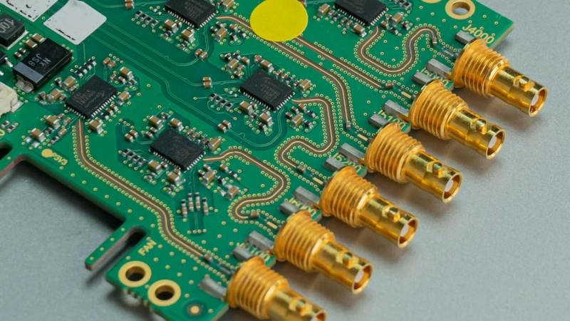
Double-sided PCBs provide engineers with a more substantial circuit substrate, being able to handle through-hole components, and the use of buried and micro-vias allows for extremely complex designs. The through-hole technology also provides PCBs with improved strength, meaning that they can be used in more demanding applications, but this also increases their cost.
Multi-layer PCBs are for advanced applications that require advanced circuitry, such as high-speed digital systems and RF amplifiers. The use of many copper layers allows for engineers to create very complex designs with controlled impedance and inductive properties, while the ability to have ground and power planes helps to improve signal integrity. However, the high layer count also makes such PCBs very expensive, and this limits their use to high-volume consumer products and high-end industrial systems. Thicker PCBs with increased copper thickness are ideal for high-current applications, such as power management and conversion, but this also increases their cost and size.
Finally, engineers should also pay attention to the dielectric used in PCBs, as this can affect signal integrity and compatibility with future PCBs. Common dielectrics include FR4 and FR1, with FR4 providing engineers with a more reliable dielectric over the long term. However, FR1 is far cheaper and easier to machine, making it ideal for prototyping.
Overall, PCBs are an amazing invention that have enabled engineers to create all kinds of advanced electronics, and the numerous variations in PCB technology allow for a wide range of different designs, from simple prototypes to the most advanced systems in active use.
What goes into PCBA?
When it comes to the production of PCBs, the assembly stage is arguably one of the most important. A PCB that has been correctly assembled will not only be of higher quality but will also be more likely to survive multiple manufacturing cycles as well as having better long-term stability.
To start, the first step in PCB assembly is to ensure that the PCB itself is free from dust and other debris. This is critical as a dirty PCB will not only have trouble adhering to solder paste during the reflow process but may also result in poor contact between components and the PCB. In addition, a clean PCB is also more likely to have uniform solder joints, which is essential for both performance and reliability.
The next step in the process involves applying solder paste to specific pads that will be connected to components. A stencil of the PCB is used that covers everything except the pads (where solder paste is needed). This also helps to prevent waste as well as ensuring uniformity in solder joints, as too much solder paste can be detrimental to a PCB.
Once the solder paste has been applied to the PCB, components are then placed onto pads using pick and place machinery. Such equipment is able to automatically read component positions of a PCB via a special footprint file, automatically feed components off of reels, and then use a specialized head that can pick out individual parts and place them onto the PCB. The high-speed nature of such equipment enables PCBs to be rapidly populated, and this in turn helps to reduce manufacturing costs.
After all the components have been placed, the PCB then goes through a reflow oven that melts the solder, simultaneously soldering the components to the PCB.
Finally, once the solder has cooled, the PCB undergoes one final cleaning stage to remove excess flux as well as debris that may have formed during the reflow stage. Overall, the entire PCB assembly process is critical, and any engineer involved with PCB design should be aware of all the steps involved.
When to use each type
When starting a new project, engineers will often start with a prototype to verify that their schematic is correct, that component values are right, and that their layout is sensible. While a prototype PCB can be ordered with all its components populated, such a PCB may not truly represent the final design (as a prototype may use larger components, larger PCB, and special development parts), potentially leading to design confusion (especially from those responsible for its mechanical design). As such, blank PCBs are useful when designing enclosures and other mechanical parts while not committing to the cost of a fully populated board.
Once a design has been proven in a prototype, it is then time to move to production. At this point, it is almost impossible to hand-solder even the smallest SMD components, meaning that engineers have no choice but to use a PCB assembly service. Such services are able to take a PCB design file, order the parts needed, and then has those parts soldered to the PCB. The end result is a fully populated PCB, ready for distribution and mass production.