Taking a design from concept to production is no small feat, but careful planning and proper use of prototyping construction methods can greatly accelerate any idea. In this series, we will develop and prototype a simple Wi-Fi IoT temperature and humidity sensor using both PCBs and laser-cut parts.
Building Workable Electronic Products Through Prototyping
Developing a product or project from the initial concept requires various stages of development, prototyping and testing. The first steps, alpha stages, generally use off-the-shelf parts, modules and rapid prototyping construction methods such as desktop 3D printers. This stage confirms the functionality of the design as well as helps determine how the final product may look, but it rarely produces a finalized design.
The secondary/beta stage creates a product that mostly resembles the final result; however, this is still a prototyping stage with many variations being developed before a design is finalized. Such variations often occur as a result of unforeseen problems with a design, including ventilation, heat dissipation, miscalculated mechanical parts, poor performance and general improvements.
In this four-part series, we will take a simple IoT device from its alpha stage to a beta and early production stage with the help of Ponoko and PCBWay services. While the device designed in these articles is not intended for commercial release, the steps we encounter, the choices of components, and the methods for prototyping enclosures and special parts will be identical to those faced during the development of commercial electronic products.
Using Ponoko And PCBWay
Before we get started, let’s introduce the two production partners used for this project: Ponoko and PCBWay.
Ponoko is an on-demand prototyping and production service that offers sheet laser cutting, engraving and bending on a range of 200+ materials including steel, brass, plastics, woods, silicone and foam. Their Bay Area U.S. facility is specifically designed for customers with smaller orders (as little as one part), offering same-day quotes and delivery. Larger orders (up to 10,000 parts) are handled by their Bay Area China facility, which offers volume discounts of up to 93%, making it ideal for the later stages of beta projects and early stages of production.
Ponoko’s laser cutting services can be used on large parts measuring up to 790 x 384 mm as well as on small parts measuring just 6 x 6 mm using materials with a thickness between 0.1 – 19.1 mm and requiring dimensional accuracy of ±0.13 mm for organic material sheets and ±0.XX mm for metal materials.
Read More – Ponoko Services
PCBWay is a PCB production and assembly service for both the maker and professional markets. Based in China, PCBWay manufactures multi-layered PCBs, cuts PCBs to any shape, manufactures individual PCBs and provides advanced manufacturing techniques including flexible PCBs. With its more recent service, PCB assembly, PCBWay sources parts, purchases and then assembles PCBs they fabricate. This service is highly ideal for modern designs that are reliant on small SMD components.
Read More – PCBWay Services
Designing An IoT Device To Measure Temperature, Humidity And Air Pressure
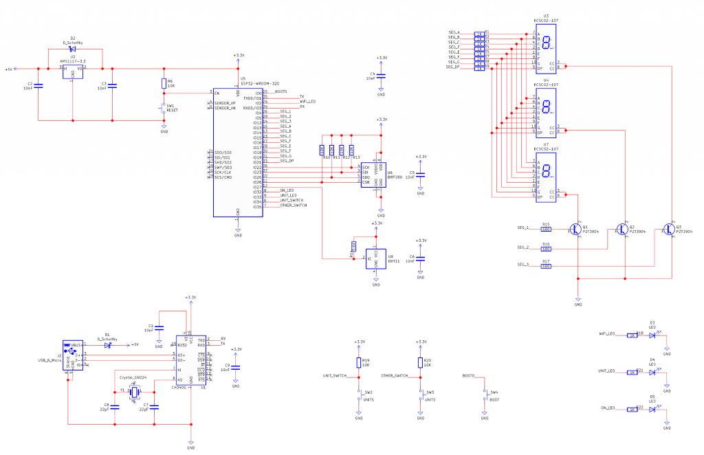
The heart of our simple IoT device is the ESP32 Wi-Fi module, provided by PCBWay. It offers wireless connectivity, has many I/O pins and comes with an RF shield to help improve its EMC performance.
Additionally, sensor capabilities are provided by two devices: the DHT11 and BMP20. The DHT11 is a one-wire device that only requires a single GPIO on the ESP32, making connections very easy. The BMP20 is an SPI device that requires four GPIO. Since the physical size of the BMP20 is so small, a PCB assembly service is the only reliable method for soldering it.
Read More – PCBWay Assembly Service
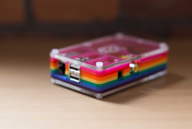
To keep circuitry simple, we’re not integrating a battery for remote operation; we’ll instead use a micro USB connector for providing power. This connector allows us to program the ESP32 with the help of a CH340 USB to UART converter. Information about the environmental conditions will be displayed on a 3×7 segment display, and several SMD LEDs will provide information on current units (°C or °F) and Wi-Fi status.
Constructed from laser-cut parts provided by Ponoko, the enclosure will display the current readings from the electronics as well as provide access to any buttons and connectors. As the product eventually becomes a commercial device, we will also consider its overall aesthetics, how easy it is to construct and the physical dimensions.
Read More – Creating laser-cut parts from various CAD software tools
The final step in the enclosure development process is choosing a production method for large-scale production. Such methods include plastic injection moulding, off-the-shelf enclosures and panel assembly.
Creating The Electronics For PCBWay
KiCad Schematic
The schematic for this IoT device is incredibly simple and takes advantage of the ESP32 modular form. Power is provided via a micro USB connection that is regulated from 5V to 3.3V using an AMS1117 (U2), and this power circuitry also integrates a special diode (D2) to protect against any voltage spikes on the ESP32 side.
The display features three, seven-segment displays that use transistors (Q1, Q2, Q3) to control which display is on at any time. By cycling through each display at high speed, we can connect all the displays to the same I/O pins and drive each display one at a time.
The connection between the ESP32 and USB is bridged using a CH340 USB to UART converter. This allows for a connected computer to program the ESP32 without needing to directly access the flash chip inside the ESP32 module. The remaining components (ESP32, DHT11 and BMP20) do not have any special requirements and are connected as needed.
The PCBWay PCB
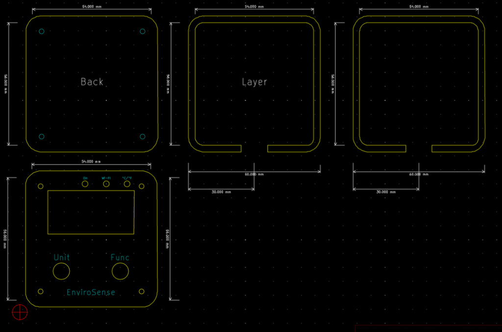
The PCB is where the design gets interesting, as this will dictate the enclosure design. While the enclosure itself influences the layout of the PCB, it is the PCB that determines the dimensions and positioning of features in the enclosure.
The first potential PCB layout puts all the components on a single PCB with the interactive parts to the left and the computational parts to the right. While this design is highly practical, it is not aesthetically pleasing, as the front panel of the design is empty on one half.
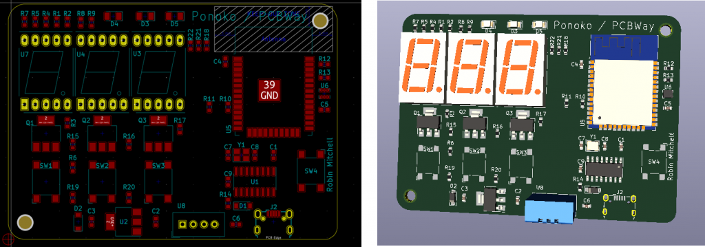
Another potential design separates the computational parts from the interactive parts into two separate PCBs. Headers attached to the display portion connect it to the computation board and allows for a much smaller device that removes the dead space on the front panel.
However, this design significantly increases the thickness of the overall design. Furthermore, the use of an additional PCB increases the costs while also requiring a more complex enclosure design. If the seven-segment displays are replaced with SMD varieties, then components could be soldered onto both sides of the PCB—but this is extraordinarily difficult to achieve.
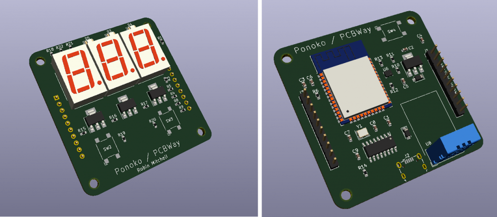
Overall, we will use the second design that features multiple layers. This is a far neater design that not only uses a smaller enclosure (despite the increase in depth) but is also partly modular, allowing for changes to be made without needing to replace the entire design.
Laser Cutting With Ponoko
Choosing A Material
Since we’re using Ponoko laser cutting services to create the enclosure, producing a 3D model is unnecessary. Laser cutters produce 2D parts that have a specific thickness; therefore, we can design our enclosure as a series of 2D parts that fit together to create a single 3D enclosure.
Before designing the enclosure, we must first pick a suitable material. This is where environmental factors become critical as some environments (such as seawater and chemical production) can harm the enclosure. As our device is a simple environmental sensor that could be subjected to wide changes in temperature and humidity, we will stick with a plastic material such as acrylic.
Read More – Ponoko Materials
Determining The Construction Method
When creating a design, there are multiple construction methods, including a layered design, box method and a pre-made enclosure with a laser-cut panel.
The layer method involves splicing an enclosure into various layers that are placed on top of each other (similar to 3D printing). However, each layer in our design can be thick (up to 10 mm), and these layers can be stacked using guiding pins before being screwed together. While this method uses a lot of layers to create the cavity for the PCB to fit within, it can be the most aesthetically pleasing.
The box method is a more practical method that is very common in maker projects. Simply put, boxes can be exploded into their individual faces with a jigsaw-like pattern appended to their edges. These individual parts are then glued together so that the jigsaw teeth lock in place. While this is practical for large boxes, small enclosures can be tricky to put together. This method is also far from a practical commercial design, meaning that a final prototype would need to use a different construction method.
The pre-made box method simply uses a commonly available project box or enclosure on the market while the faceplate is replaced with a laser-cut design. This design method is a quick option to create a product and can sometimes be the final product (as such enclosures are available in large quantities). However, such a design is far from professional and can make a product look underdeveloped.
Finalizing The Design
Our design uses the layer method, as this creates a compact design that looks similar to the final design. Another advantage of the layer design is that we can use different materials at different layers; in the case of this project, we can make the front panel in aluminum for a metallic face finish (similar to Apple products) while having a plastic backing.
As laser-cut designs are 2D, we can easily design our enclosure in KiCad’s PCB development tool, which exports SVG files that are easy to upload to Ponoko’s website for instant quoting. Furthermore, we can import other PCBs into our design to easily match our enclosure design with our PCB design.
Prototyping: Truly Understanding If The Design Works
With the designs complete, it is time to order parts for manufacturing. While we know that the circuit functions properly from earlier testing (not discussed here), the final design could be met with challenges that have not been currently foreseen (such as incorrect placement of parts or improper trace widths). Furthermore, our PCB may not fit our enclosure correctly, or the use of layers may prove to be too challenging.
This is why creating a prototype is essential; having a physical product is the only way to truly understand if a design will work or not.
In the next article, we will look at ordering PCBs and PCB assembly from PCBWay, ordering laser-cut parts from Ponoko and the challenges that will follow.

1 Comment
hi there, i recently done an online quote which came back in $US.Do I have to convert this myself or did I miss a button somewhere to change into NZ dollars.
cheers
Comments are closed.